PCB electrical measurement technology analysis
First, electrical test
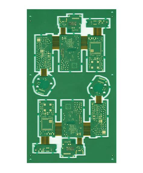
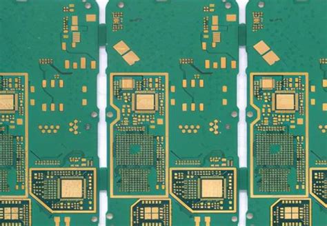
PCBs in the production process, it is inevitable that due to external factors caused by short circuit, open circuit and leakage and other electrical defects, coupled with the continuous evolution of PCB to high density, fine pitch and multi-level evolution, if not in time to bad board Screening out, and letting it flow into the process, is bound to cause more costly waste, so in addition to process control improvements, improving the test technology can also provide PCB manufacturers with reduced scrap rate and improve product yield solutions .
In the production process of electronic products, due to the loss caused by defects, there are different degrees in various stages. The earlier the discovery, the lower the cost of remediation.
“The Rule of 10’s” is a remedial cost that is often used to evaluate PCBs found to be defective at various stages of processing. For example, if empty circuit boards are manufactured, if the circuit breakers in the circuit board can be detected in real time, it is usually sufficient to repair the circuit breakers, or at least one empty board is lost. However, if a circuit breaker cannot be detected, the board is shipped. After the downstream assembly companies completed the parts installation and remelted the furnace and IR, they were found to have broken circuit at this time. The general downstream assembler would ask the empty plate manufacturing company to claim compensation for part costs and heavy labor costs. , inspection fees, etc. If, unfortunately, the test of the defective board is still undetected by the assembly industry, and the product is entered into the entire system, such as computers, mobile phones, and auto parts, the loss that will be discovered at this point will be detected in a timely manner. A hundredfold, a thousand times, or even more. Therefore, for the PCB industry, the electrical test is for the early detection of board defects.
Downstream players will usually require PCB manufacturers to conduct 100% electrical tests. Therefore, they will agree with the PCB manufacturers on test conditions and test methods. Therefore, both parties will clearly define the following items:
1, test data sources and formats
2, test conditions, such as voltage, current, insulation and connectivity
3, equipment production methods and selection
4, test chapter
5, patch specifications
In the PCB manufacturing process, there are three stages that must be tested:
1, after the inner layer is etched
2, After the outer layer is etched
3, finished product
There are usually 2 to 3 100% tests at each stage, and the bad plates are screened for rework. Therefore, the test station is also the best data collection source for the analysis of process problems. Through the statistical results, the percentage of open circuit, short circuit, and other insulation problems can be obtained. After heavy industry, the test is performed again. After the data is collected, the quality control method is used to find The root cause of the problem is solved.
Second, electrical testing methods and equipment
The electrical test methods are: Dedicated, Universal Grid, Flying Probe, E-Beam, Conductive Fabric, Capacity And brush test (ATG-SCAN MAN), the most commonly used equipment there are three, namely, special test machine, general purpose test machine and flying probe tester. In order to better understand the functions of various devices, the following will compare the characteristics of the three major devices.
1. Dedicated test
The reason why a dedicated type of test is dedicated is that the fixture used (Fixture, such as a dial for electrical testing on a circuit board) is only applicable to one item number, and boards with different item numbers cannot be tested. And can not be recycled. As for the number of test points, the single panel can be tested at 10,240 points or 8,192 points on both sides. In terms of test density, the thickness of the probe head is more suitable for the board above the pitch.
2. Universal Grid Testing
The basic principle of general-purpose testing is that PCB layout is based on a grid. Generally speaking, the line density refers to the distance of the grid, which is the pitch (partially, the hole density can also be used to represent ), and general-purpose testing is based on this principle, according to the hole position with a G10 substrate for the Mask, only in the hole position of the probe can pass through the Mask for electrical measurement, so the fixture is simple and rapid, and exploration The needle can be reused. General-purpose type test has a large number of standard grid fixed large-scale dials, which can be used to produce movable probe dials according to different item numbers. When mass production is changed, the active dials can be changed, and different batch numbers can be produced. test. In addition, in order to ensure that the completed PCB board line system is unobstructed, it is necessary to perform Open/Short electrical test on the board using a specific contact pin on a general-purpose electrical tester that uses high-voltage (for example, 250V) multi-points. This general-purpose tester is called Automatic Test Equipment (ATE).
The number of general-purpose test points is usually more than 10,000 points, and the test of the test density at or is called the on-grid test. If it is applied to high-density boards, the space is too dense and has been separated from the on-grid design, so it belongs to off-grid. For testing, its fixtures must be specially designed. Generally, the test density of general-purpose tests can reach QFP.
3, Flying Probe (Flying Probe) test
The principle of the flying probe test is very simple. Only two probes are needed to move x, y, and z to test the two ends of each line one by one. Therefore, no expensive fixtures need to be fabricated separately. However, because it is an end point test, the speed is very slow, about 10~40 points/sec, so it is more suitable for samples and small-scale production; in the test density, the flying probe test can be applied to very high density boards (), such as MCM.