PCB electromagnetic compatibility design and heat dissipation
PCB Introduction
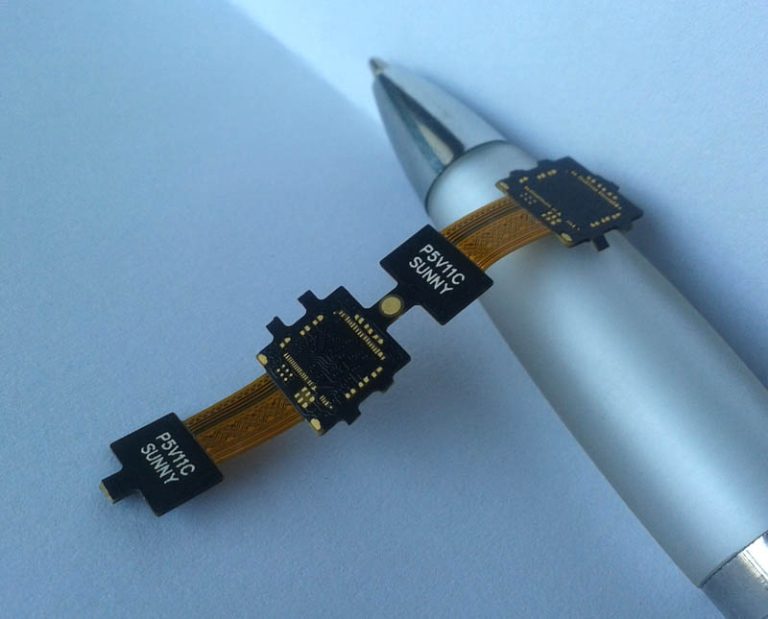
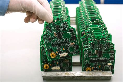
PCB, Chinese name for printed circuit board, also known as printed circuit board, printed circuit board, is an important electronic component, a support for electronic components, and a provider of electrical connections for electronic components. Because it is made using electronic printing technology, it is called a “printed” circuit board.
Classification according to the number of circuit layers:
divided into single-sided board, double-sided board and multi-layer board.
Common multi-layer boards are generally 4-layer boards or 6-layer boards, and complex multi-layer boards can reach more than ten layers.
PCB boards have the following three main types of division:
Single-sided board
On the most basic PCB, the parts are concentrated on one side of the single-sided board, and the wires are concentrated on the other side. Because the wires only appear on one side, this type of PCB is called a single-sided board. Because single-sided boards have many strict restrictions on designing circuits, only early circuits use this type of board.
Double-sided board
Double-sided board This type of circuit board has wiring on both sides, but to use the wires on both sides, there must be appropriate circuit connections between the two sides. This “bridge” between circuits is called a guide hole. A via is a small hole filled or coated with metal on a PCB, which can be connected to the wires on both sides. Because the area of a double-sided board is twice that of a single-sided board, and because the wiring can be interlaced, it is more suitable for use in more complex circuits than single-sided boards.
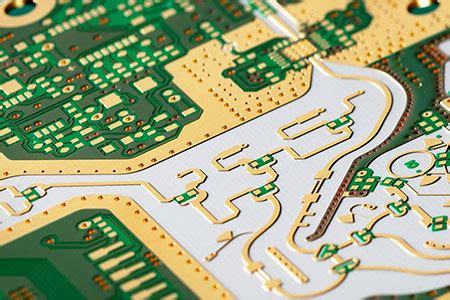
Multilayer board
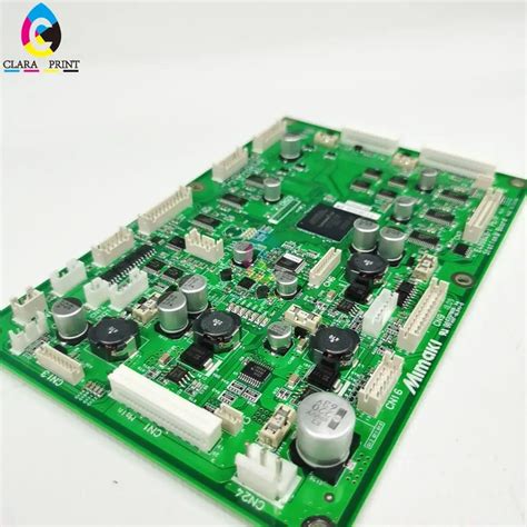
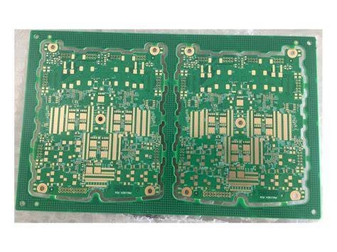
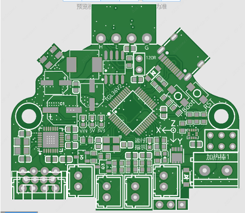
In order to increase the area that can be wired, multilayer boards use more single- or double-sided wiring boards. A printed circuit board with one double-sided board as the inner layer and two single-sided boards as the outer layer, or two double-sided boards as the inner layer and two single-sided boards as the outer layer, is alternately connected through a positioning system and insulating adhesive materials, and the conductive patterns are interconnected according to the design requirements. The printed circuit board becomes a four-layer or six-layer printed circuit board, also known as a multilayer printed circuit board. The number of layers on the board represents the number of independent wiring layers, usually an even number of layers, and includes the two outermost layers. Most motherboards have a structure of 4 to 8 layers, but technically, it is theoretically possible to achieve a PCB board with nearly 100 layers. Most large supercomputers use motherboards with quite a few layers, but because such computers can be replaced by clusters of many ordinary computers, super-multilayer boards have gradually fallen out of use. Because the layers in the PCB are tightly combined, it is generally not easy to see the actual number, but if you look closely at the motherboard, you can still see it.
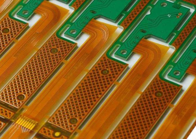
According to the soft and hard classification, it is divided into ordinary circuit boards and flexible circuit boards.
PCB is the platform for the operation of circuit components in electronic equipment. It provides electrical connections between circuit components, and its performance is directly related to the quality of electronic equipment. With the rapid development of microelectronics technology and the improvement of circuit integration, the density of components on PCB boards is getting higher and higher, and the system is working faster and faster, which makes PCB electromagnetic compatibility design more and more important and becomes the key to the stable and normal operation of a circuit system.
2 Common electromagnetic interference in PCB
There are two ways to solve the electromagnetic compatibility problem in PCB design: active reduction and passive compensation. For this reason, the interference source and propagation path of electromagnetic interference must be analyzed. The electromagnetic interference that usually exists in PCB design includes: conducted interference, crosstalk interference and radiated interference.
2.1 Conducted interference
Conducted interference mainly affects other circuits through wire coupling and common mode impedance coupling. For example, if noise enters a system through the power supply circuit, all circuits using the power supply will be affected. Figure 1 shows that noise is coupled through common mode impedance. Circuit 1 and Circuit 2 use a wire to obtain the power supply voltage and ground loop. If the voltage of Circuit 1 suddenly needs to increase, the voltage of Circuit 2 will inevitably decrease due to the shared power supply and the impedance between the two loops.
2.2 Crosstalk Interference
Crosstalk interference is a signal line interfering with another adjacent signal path. It usually occurs on adjacent circuits and conductors, and is characterized by the mutual capacitance and mutual inductance of the circuits and conductors. For example, a stripline on a PCB carries a low-level signal. When the parallel wiring length exceeds 10cm, crosstalk interference will occur. Since crosstalk can be caused by electric fields through mutual capacitance and magnetic fields through mutual inductance, when considering the crosstalk problem on PCB striplines, the most important issue is to determine which of the electric field and magnetic field coupling is the main factor.
2.3 Radiated Interference
Radiated interference is interference introduced by the radiation of electromagnetic waves in space. Radiated interference in PCB is mainly common-mode current radiation interference between cables and internal traces. When electromagnetic waves are radiated to the transmission line, field-to-line coupling problems will occur. The distributed small voltage source caused along the line can be decomposed into common mode and differential mode components. Common mode current refers to the current with very small amplitude difference and the same phase on two wires, while differential mode current refers to the current with equal amplitude and opposite phase on two wires.
3 Electromagnetic compatibility design of PCB
With the increasing density of electronic components and circuits on PCB boards, in order to improve the reliability and stability of the system, corresponding measures must be taken to make the design of PCB boards meet the requirements of electromagnetic compatibility and improve the anti-interference performance of the system.
3.1 Selection of PCB boards
In PCB board design, crosstalk occurs between signals on adjacent transmission lines due to mutual coupling of electromagnetic fields. Therefore, when designing the electromagnetic compatibility of PCB, the size of PCB should be considered first. If the size of PCB is too large and the printed line is too long, the impedance will inevitably increase, the anti-noise ability will decrease, and the cost will also increase. If the size of CB is too small, crosstalk is likely to occur between adjacent transmission lines, and the heat dissipation performance is not good.
The number of layers of PCB board is determined according to comprehensive factors such as the type of power supply and ground, the density of signal lines, signal frequency, the number of signals required for special wiring, peripheral factors, cost price, etc. To meet the strict EMC indicators and consider the manufacturing cost, appropriately increasing the ground plane is one of the best methods for PCB EMC design. For the power layer, the needs of multiple power supplies can generally be met by dividing the inner power layer. However, if multiple power supplies are required and they are intertwined, two or more power planes must be considered. For the signal layer, in addition to considering the routing density of the signal line, from the perspective of EMC, it is also necessary to consider the shielding or isolation of key signals to determine whether to increase the number of corresponding layers.
3.2 PCB board layout design
PCB layout should generally follow the following principles:
(1) Try to shorten the connection between high-frequency components to reduce their distributed parameters and mutual electromagnetic interference. Components that are easily interfered with should not be too close, and inputs and outputs should be kept as far away as possible.
(2) Some components or wires may have higher voltages, and the distance between them should be increased to avoid discharge and accidental short circuits.
(3) Devices with high heat generation should leave space for heat sinks, and should even be installed on the bottom plate of the whole machine to facilitate heat dissipation. Thermistors should be kept away from heating components.
(4) Arrange the positions of each functional unit according to the flow of the circuit, so that the layout is convenient for signal flow and the signal can maintain the same direction as much as possible.
(5) Take the core component of each functional module as the center and arrange it around it to minimize and shorten the lead and connection length between components.
(6) Comprehensively consider the distribution parameters between components. Arrange the components in parallel as much as possible, which is not only conducive to enhancing the anti-interference ability, but also beautiful in appearance and easy to mass produce.
3.3 Layout design of components
Compared with discrete components, integrated circuit components have the advantages of good sealing, fewer solder joints and low failure rate, and should be used first. At the same time, the selection of devices with slower signal slope can reduce the high-frequency components generated by the signal. The full use of surface mount components can shorten the connection length, reduce impedance and improve electromagnetic compatibility.
When arranging components, first group them in a certain way, put the same group together, and arrange incompatible devices separately to ensure that the components do not interfere with each other in space. In addition, components with heavier weight should be fixed with brackets.
For heat dissipation of electronic components such as PCB circuit boards and MOS tubes, it is recommended to choose thermal conductive silicone sheets!
Main products: thermal conductive silicone sheets, thermal conductive grease, synthetic graphite sheets, natural graphite sheets, thermal conductive mud, thermal conductive double-sided tape, thermal conductive silicone cloth and other thermal conductive heat dissipation materials;
Specialized in solving the heat dissipation problems of electronic components such as notebooks, computers, mobile phones, LEDs, semiconductors, power supplies, electric vehicles, etc., thermal conductive material manufacturer Hefei Aoqi Electronic Technology Co., Ltd.,