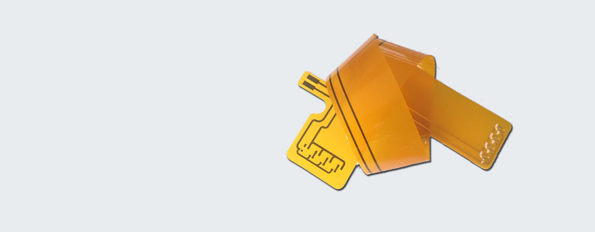
Bga on flex pcb
With the continuous enhancement of electronic device functionalities, their sizes have been continuously shrinking.
In order to meet the functional requirements of these smaller devices, component packaging technologies have also been advancing.
Since the late 1980s, Ball Grid Array (BGA) has emerged as one of the most popular packaging technologies,
making significant contributions to meet this demand.
They provide higher interconnect density compared to through-hole PGA and surface-mount QFP,
with comparable costs and without the manufacturing issues associated with these packaging types.
Since then, their popularity has been continuously increasing,
and they have become the default packaging for high pin-count integrated circuits such as microprocessors and storage devices.
BGA, short for Ball Grid Array, is a type of surface-mount packaging (chip carrier) used for integrated circuits.
Traditionally, conventional surface-mount packages use side connections to achieve limited pin connection area.
In contrast, BGA packages utilize bottom connections, offering larger connection space,
enabling high-density PCBs and high-performance electronic products.
BGA packages come in various pin pitch specifications such as 1.27mm, 1.0mm, 0.8mm, 0.75mm, 0.65mm, 0.5mm, 0.4mm, and more.

Advantages of BGA Package
Efficient utilization of PCB space: Using BGA packages means fewer components involved and a smaller footprint,
which helps save space on custom PCBs and greatly improves PCB space efficiency.
Enhanced thermal and electrical performance: Due to the smaller size of PCBs with BGA packaging, heat dissipation becomes easier.
When the silicon chip is mounted on the top, most of the heat can transfer downward through the ball grid array.
When the silicon chip is mounted on the bottom, the backside of the die is connected to the top of the package,
which is considered one of the best cooling methods.
BGA packages have no bendable or breakable pins, making them stable enough to ensure electrical performance on a large scale.
Improved soldering process and increased production yield: Most BGA package solder balls are relatively large,
making large-area soldering easier and more convenient, thereby increasing PCB manufacturing speed and yield.
The larger solder balls also facilitate rework.
Minimal damage to leads: BGA leads consist of solid solder balls, which are less prone to damage during use.
Cost reduction: All of the above advantages contribute to cost reduction.
Efficient utilization of PCB space provides opportunities for material savings,
while improved thermal and electrical performance helps ensure the quality of electronic components and reduces the chances of defects.
Commonly Used BGA PackageTypes
Based on the substrate and other materials used, Ball Grid Array (BGA) packaging comes in various subtypes.
All these subtypes use solder balls to connect the package to the circuit board. Let’s introduce some common types of BGA packages.
- Plastic BGA (PBGA):
- PBGA typically uses BT resin/glass laminate as the substrate and plastic as the packaging material.
Solder balls can be either leaded or lead-free. No additional solder is required to connect the solder balls to the package. - Ceramic BGA (CBGA):
- CBGA is a long-standing BGA packaging type, different from PBGA and TBGA.
It uses a multilayer ceramic substrate as the base material. - The metal lid is soldered to the substrate with packaging solder to protect the chip, leads, and solder balls. Eutectic solder material is used for the solder balls.
- Tape BGA (TBGA):
- TBGA is a structure with cavities. There are two interconnection methods between the chip and the substrate:
reverse bonding and wire bonding. - Micro BGA (uBGA):
- uBGA is a BGA chip packaging technology developed by Tessera, primarily used for high-frequency operation in RDRAM.
This technology allows for smaller chip sizes, improved heat dissipation, and increased data density in memory modules. - Fine-Pitch BGA (FBGA):
- Also known as Chip Scale Package (CSP), FBGA is a pin grid array structure with solder balls on the bottom, making the required installation area close to the chip size.
- This high-density, compact, and flat package technology is well-suited for designing compact handheld consumer electronic devices such as personal digital assistants, mobile phones, camcorders, and digital cameras.

the role of bga on flex pcb
The role of BGA (Ball Grid Array) on flex PCB (Flexible Printed Circuit Board) is to provide a compact and high-density packaging solution for integrated circuits while also allowing flexibility in the circuit board.
BGA is a surface-mount packaging technology that uses a grid of solder balls to connect the IC to the PCB.
BGA on flex PCB is used in various applications where space is limited, and flexibility is required.
For instance, in portable electronic devices such as smartphones, tablets, and wearables,
where the PCB needs to be flexible to accommodate the device’s shape and size.
The BGA’s compact size and high pin density make it an ideal choice for small and complex electronic devices.
Additionally, the BGA’s solder balls provide a strong and reliable connection to the flexible substrate, ensuring the circuit board’s durability.
In summary, the role of BGA on flex PCB is to provide a compact, high-density, and flexible packaging solution for integrated circuits,
making it an ideal choice for small and complex electronic devices.