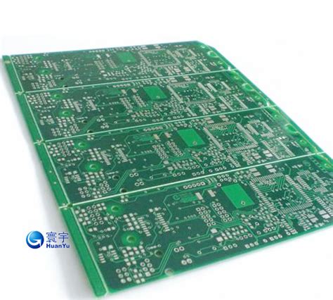
Pcb electronics
Designing High-Performance PCBs: Best Practices and Tips
Designing high-performance printed circuit boards (PCBs) is a critical task that demands meticulous attention to detail and a deep understanding of both the theoretical and practical aspects of electronics. The process begins with a clear definition of the requirements and constraints, which include the electrical, mechanical, and thermal specifications of the final product. To achieve optimal performance, designers must consider several best practices and tips that can significantly enhance the functionality and reliability of the PCB.
One of the fundamental aspects of high-performance PCB design is the layout.
A well-thought-out layout can minimize signal interference, reduce noise, and ensure efficient power distribution. It is essential to place components strategically to shorten the length of critical signal paths. This not only reduces the potential for signal degradation but also minimizes the risk of electromagnetic interference (EMI). Additionally, designers should pay close attention to the placement of decoupling capacitors near power pins to filter out noise and stabilize the power supply.
Transitioning to the topic of trace routing, it is crucial to maintain consistent trace widths and avoid sharp angles, which can cause signal reflections and impedance mismatches.
Differential pairs, commonly used for high-speed signals, should be routed together with controlled impedance to maintain signal integrity. Furthermore, designers should implement proper grounding techniques, such as using a solid ground plane, to provide a low-impedance return path for signals and reduce the risk of ground loops.
Thermal management is another critical consideration in high-performance PCB design.
As electronic components become more powerful, they also generate more heat, which can adversely affect performance and reliability. Effective thermal management strategies include the use of thermal vias, heat sinks, and proper component spacing to facilitate heat dissipation. Additionally, designers should consider the thermal properties of the PCB materials and select those with high thermal conductivity to enhance heat transfer.
Incorporating design for manufacturability (DFM) principles is also essential to ensure that the PCB can be produced efficiently and cost-effectively.
This involves considering the capabilities and limitations of the manufacturing process, such as minimum trace widths, spacing, and hole sizes. By adhering to DFM guidelines, designers can avoid common pitfalls that may lead to production delays or increased costs.
Signal integrity analysis is another vital aspect of high-performance PCB design.
Tools such as simulation software can help identify potential issues related to signal integrity, such as crosstalk, reflections, and ringing. By performing these analyses early in the design process, designers can make necessary adjustments to mitigate these issues and ensure reliable signal transmission.
Moreover, designers should not overlook the importance of thorough testing and validation.
Prototyping and testing the PCB under real-world conditions can reveal potential issues that may not be apparent during the design phase. This iterative process allows for fine-tuning and optimization of the design to achieve the desired performance.
In conclusion, designing high-performance PCBs requires a comprehensive approach that encompasses careful layout planning, precise trace routing, effective thermal management, adherence to DFM principles, rigorous signal integrity analysis, and thorough testing. By following these best practices and tips, designers can create PCBs that meet the stringent demands of modern electronic applications, ensuring both functionality and reliability.

The Future of PCB Technology: Innovations and Trends
The future of PCB technology is poised for remarkable advancements, driven by continuous innovations and emerging trends that promise to revolutionize the electronics industry. As the backbone of modern electronic devices, printed circuit boards (PCBs) are integral to the functionality and performance of a wide array of applications, from consumer electronics to industrial machinery. Consequently, the evolution of PCB technology is closely monitored by industry experts and stakeholders who are keen to leverage new developments to enhance product capabilities and efficiency.
One of the most significant trends shaping the future of PCB technology is the miniaturization of electronic components.
As devices become increasingly compact, there is a growing demand for smaller, yet more powerful, PCBs. This trend is particularly evident in the consumer electronics sector, where smartphones, wearables, and other portable devices require highly efficient and densely packed circuit boards. To meet these demands, manufacturers are exploring advanced materials and fabrication techniques, such as high-density interconnect (HDI) technology, which allows for more intricate and compact designs without compromising performance.
In addition to miniaturization, the integration of flexible and rigid-flex PCBs is gaining traction.
These innovative designs offer greater versatility and durability, making them ideal for applications that require bending or folding, such as medical devices and aerospace components. Flexible PCBs, made from materials like polyimide, can withstand harsh environments and mechanical stress, thereby extending the lifespan and reliability of electronic devices. As a result, the adoption of flexible and rigid-flex PCBs is expected to grow, driven by the need for more adaptable and resilient electronic solutions.
Another key innovation in PCB technology is the incorporation of advanced materials, such as graphene and other nanomaterials.
These materials exhibit exceptional electrical, thermal, and mechanical properties, which can significantly enhance the performance of PCBs. For instance, graphene’s high conductivity and flexibility make it an ideal candidate for next-generation PCBs that require efficient heat dissipation and robust electrical performance. As research and development in nanomaterials continue to progress, it is anticipated that these advanced materials will play a crucial role in the future of PCB technology.
Moreover, the rise of the Internet of Things (IoT) and the proliferation of connected devices are driving the need for more sophisticated and intelligent PCBs.
IoT devices often require complex circuitry and advanced communication capabilities to function effectively. To address these requirements, PCB manufacturers are incorporating embedded components, such as sensors and microcontrollers, directly into the circuit board. This integration not only reduces the overall size and weight of the device but also enhances its functionality and connectivity.
Sustainability is another important consideration in the future of PCB technology.
As environmental concerns become more pressing, there is a growing emphasis on developing eco-friendly manufacturing processes and materials. Innovations such as biodegradable PCBs and the use of recyclable materials are being explored to minimize the environmental impact of electronic waste. Additionally, advancements in additive manufacturing, or 3D printing, offer the potential for more efficient and sustainable PCB production methods, reducing material waste and energy consumption.
In conclusion, the future of PCB technology is characterized by a convergence of miniaturization, advanced materials, flexible designs, IoT integration, and sustainability. These innovations and trends are set to transform the electronics industry, enabling the development of more powerful, versatile, and environmentally friendly devices. As the demand for sophisticated electronic solutions continues to grow, the ongoing evolution of PCB technology will play a pivotal role in shaping the next generation of electronic products and applications.
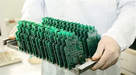
Common PCB Manufacturing Mistakes and How to Avoid Them
Printed Circuit Boards (PCBs) are the backbone of modern electronic devices, providing the necessary pathways for electrical currents to flow between various components. However, the process of manufacturing PCBs is fraught with potential pitfalls that can compromise the functionality and reliability of the final product. Understanding common PCB manufacturing mistakes and how to avoid them is crucial for ensuring high-quality outcomes.
One prevalent mistake in PCB manufacturing is the improper design of the board layout.
A poorly designed layout can lead to issues such as signal interference, inadequate power distribution, and thermal management problems. To avoid these issues, it is essential to follow best practices in PCB design, such as maintaining proper spacing between components, using appropriate trace widths, and ensuring adequate grounding. Additionally, employing design rule checks (DRCs) can help identify potential layout issues before the manufacturing process begins.
Another common error is the selection of inappropriate materials.
The choice of substrate material, copper thickness, and solder mask can significantly impact the performance and durability of the PCB. For instance, using a substrate material with poor thermal conductivity can lead to overheating and eventual failure of the board. To mitigate this risk, it is important to select materials that are compatible with the intended application and operating environment of the PCB. Consulting with material suppliers and leveraging industry standards can provide valuable guidance in making informed material choices.
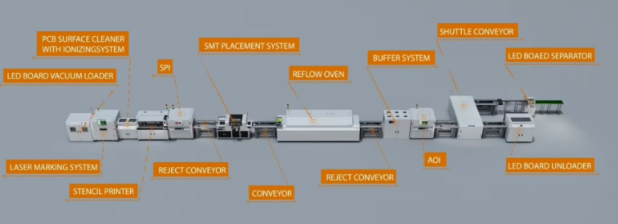
Soldering defects are also a frequent issue in PCB manufacturing.
Problems such as cold joints, solder bridges, and insufficient solder can result in unreliable connections and intermittent failures. To prevent these defects, it is crucial to implement proper soldering techniques and quality control measures. This includes using the correct solder paste, maintaining appropriate reflow oven profiles, and conducting thorough inspections of solder joints. Automated optical inspection (AOI) and X-ray inspection systems can be particularly effective in identifying soldering defects that may not be visible to the naked eye.
Furthermore, inadequate testing and inspection procedures can lead to undetected faults in the final product
. Skipping or rushing through testing phases can result in boards that fail in the field, leading to costly recalls and damage to the manufacturer’s reputation. To avoid this, it is essential to implement comprehensive testing protocols, including in-circuit testing (ICT), functional testing, and burn-in testing. These tests help ensure that the PCB performs as expected under various conditions and can withstand the rigors of real-world use.
In addition to these technical considerations, communication and collaboration between design and manufacturing teams play a critical role in preventing PCB manufacturing mistakes.
Misunderstandings or lack of communication can lead to errors such as incorrect component placement, mismatched footprints, and incompatible design specifications. To foster effective collaboration, it is important to establish clear communication channels and involve all relevant stakeholders throughout the design and manufacturing process. Regular design reviews and feedback sessions can help identify and address potential issues early on.
In conclusion, avoiding common PCB manufacturing mistakes requires a combination of meticulous design practices, careful material selection, rigorous quality control, and effective communication. By adhering to these principles, manufacturers can produce reliable and high-performing PCBs that meet the demands of modern electronic applications. Investing time and resources in these areas not only enhances the quality of the final product but also contributes to the overall success and reputation of the manufacturing organization.
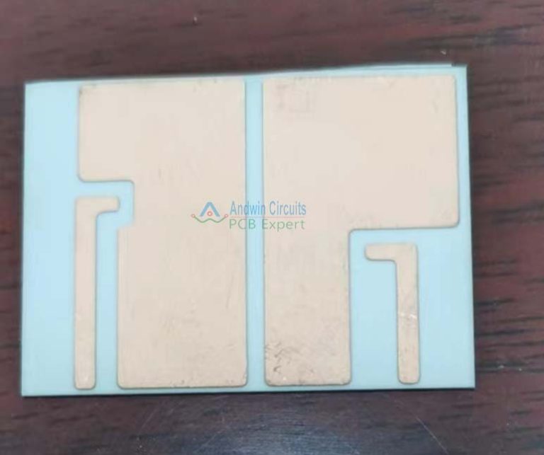
Understanding PCB Materials: Choosing the Right Substrate for Your Project
Printed Circuit Boards (PCBs) are the backbone of modern electronic devices, providing the necessary platform for mounting and interconnecting various electronic components. The choice of substrate material for a PCB is a critical decision that can significantly impact the performance, reliability, and cost of the final product. Understanding the different types of PCB materials and their properties is essential for selecting the right substrate for your project.
One of the most commonly used materials for PCB substrates is FR-4, a composite material made of woven fiberglass cloth with an epoxy resin binder.
FR-4 is favored for its excellent mechanical strength, good electrical insulation properties, and relatively low cost. It is suitable for a wide range of applications, from consumer electronics to industrial equipment. However, FR-4 may not be the best choice for high-frequency applications due to its relatively high dielectric constant and loss tangent.
For high-frequency and high-speed digital applications, materials with lower dielectric constants and loss tangents are preferred.
Rogers materials, such as RO4000 and RO3000 series, are popular choices in these scenarios. These materials offer superior electrical performance, making them ideal for RF and microwave circuits. Additionally, they exhibit excellent thermal stability, which is crucial for maintaining performance in demanding environments. However, Rogers materials are generally more expensive than FR-4, which can be a consideration for cost-sensitive projects.
Another important category of PCB materials is polyimide, known for its exceptional thermal stability and flexibility.
Polyimide substrates are often used in flexible PCBs, which are essential for applications requiring bending and folding, such as wearable electronics and medical devices. The high thermal resistance of polyimide also makes it suitable for high-temperature applications, including aerospace and automotive electronics. Despite its advantages, polyimide is more costly than FR-4 and can be more challenging to process.
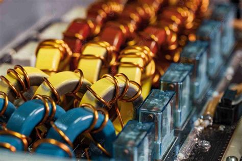
Metal-core PCBs (MCPCBs) are another option, particularly for applications requiring efficient heat dissipation.
These substrates incorporate a metal layer, typically aluminum or copper, to enhance thermal conductivity. MCPCBs are commonly used in LED lighting, power supplies, and other high-power applications where managing heat is critical. The metal core helps to dissipate heat away from sensitive components, improving reliability and extending the lifespan of the device. However, the inclusion of a metal layer can increase the weight and cost of the PCB.
Ceramic substrates, such as alumina and aluminum nitride, offer excellent thermal conductivity and electrical insulation properties.
These materials are often used in high-power and high-frequency applications, including RF amplifiers and power modules. Ceramic substrates can operate at higher temperatures and provide better thermal management than traditional materials. However, they are more brittle and expensive, which can limit their use to specialized applications.
In conclusion, selecting the right PCB substrate material involves balancing various factors, including electrical performance, thermal management, mechanical properties, and cost. FR-4 remains a versatile and cost-effective choice for many applications, while materials like Rogers, polyimide, metal-core, and ceramics offer specialized benefits for specific needs. By carefully considering the requirements of your project and the properties of different materials, you can make an informed decision that ensures optimal performance and reliability of your electronic device.