PCB electroplating simulation for zero experience
PCBs are the heart of almost all electronic products, carrying the components and copper wires that enable their functions. Electroplating is often included in the manufacturing process, and electroplating varies from design to design. This forces simulation and optimization engineers to constantly create new models. What if most of this work could be handed over to the designers, engineers, and technicians who design and manufacture PCBs to simulate electroplating themselves? Here is how to do it.
Custom Electroplating Simulation App Application
Electroplating apps can be customized using the App Builder and the Electroplating Module in COMSOL Multiphysics version 5.0. With it, PCB designers can use simulation to analyze many factors in the design and manufacturing process. They can determine whether a design can meet copper wire specifications, evaluate the performance of such devices, and estimate the manufacturing cost of the electroplating process without having to have knowledge of electroplating.
Design Challenges in Electroplated Copper Patterns
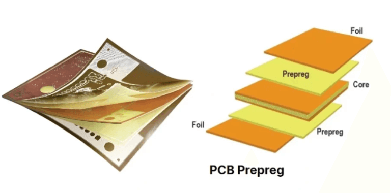
Common PCBs use one or more layers of copper wire to connect active and passive devices on the board. On the other hand, in more advanced PCBs, copper patterns are electroplated to create the circuits. Before the actual electroplating begins, a patterned insulating film should be prepared on the PCB. This process is achieved in several steps.
Preparing a patterned insulating film on the PCB:
The first step is to plate a thin conductive copper seed layer on the PCB. Next, the surface of the PCB needs to be coated with a photoresist (photosensitive polymer film), a process commonly known as photolithography. This process involves exposing the photoresist covered with a patterned mask to ultraviolet light, which dissolves the exposed areas. The result is a PCB with a patterned insulating film and a seed layer at the bottom of the pattern exposed.
PCB electroplating simulation with zero experience
The seed layer is plated on the PCB (left). The PCB pattern is drawn using photoresist by photolithography (right).
During the electroplating process, the PCB and the copper anode (such as a solid copper strip) are immersed in a plating tank containing an electrolyte containing sulfuric acid and copper sulfate. A voltage is applied between the anode and the seed layer cathode, which causes an electrochemical reduction reaction in which copper ions are reduced to the copper metal plated (deposited) on the seed layer. Over time, the thickness of the coating is directly proportional to the rate of the electrochemical reaction, which is determined by the current density at different locations in the seed layer. As a result, the patterned photoresist cavities are filled with solid copper. The plating rate can be maintained by controlling the average current density (i.e., the total current size in the patterned area to be plated).
Finally, the remaining photoresist is removed and the thin seed layer is etched to separate the different copper-plated lines.
… The electric field in the electrolyte concentrates on conductive patterns surrounded by large insulating areas and near the edges of the PCB. The non-uniformity of the electric field produces higher local current density on the cathode surface in these areas, an effect often called current crowding. Over time, the thickness of the plating is proportional to the current density, which causes undesirable variations in the thickness of the copper lines in the PCB. This means that the resistance between the copper lines at different locations on the PCB will vary. When the PCB is used in electronic devices, this thickness variation can be the root cause of performance problems or, in the worst case, device failure.
PCB electroplating simulation with zero experience
In the step of electroplating copper patterns, the PCB and copper anodes are immersed in the plating tank (electrolyte) (left). After applying a voltage between the anode and the PCB, copper is deposited and forms a conductor pattern. The electric field from the anode to the conductive part of the PCB is crowding near large insulating areas and the edges of the PCB (shown as a colored electric field line diagram in the left figure). This results in higher local copper thickness in these areas (see the red part in the wire pattern on the right).
Simulation and optimization in the design stage
To avoid performance degradation or device failure in the operation of electronic devices, copper wire circuits must meet a set of thickness uniformity specifications. Typically, printed circuit board designers rely on simple design rules such as maximum and minimum line widths, spacing, and pattern density. However, through electroplating simulation, it is possible to more accurately calculate the expected copper layer thickness variation that can be achieved. With this information, the design can be modified early without waiting for prototype results.
To reduce current crowding, “dummy” pattern designs can be added to locations where large insulating areas are usually located. At this time, the dummy pattern will accept part of the current, which will reduce the high current density in the actual wiring pattern. Some areas of the dummy pattern will still have higher current density, but since it is not part of the actual wiring, it does not matter. Through simulation, it is quick and easy to redesign and calculate the thickness uniformity obtained by different pattern layouts.

PCB electroplating simulation with zero experience
To reduce the thickness variation of copper patterns, dummy patterns can be added to locations where large insulating areas are usually located. In the left image, the red areas show the thicker copper pattern near the insulating area. The right image shows how to add dummy patterns to reduce the thickness variation in the copper wiring pattern.
Another step to reduce thickness variation is related to the electroplating tank setup.
To reduce the current crowding effect at the edge, a device called an aperture can be used.
An aperture is essentially an insulating shield with an opening that is placed between the copper anode and the PCB in the electroplating tank. The size of the aperture opening must be smaller than the size of the PCB to reduce current crowding at the edge. Beyond that, it is difficult to estimate the optimal size and placement of the aperture.
Fortunately, optimization can be done quickly and easily through simulation. The figure below simulates an aperture with a rectangular opening. The length and width of the aperture opening and its placement in the electroplating tank are optimized to minimize the thickness variation on the PCB.
PCB electroplating simulation with zero experience
To avoid the crowding effect near the edge of the PCB (as shown on the left), an aperture with an opening, i.e. an insulating shield, can be placed between the anode and the electroplating tank. The image to the right shows the aperture opening size and placement in the plating tank optimized for minimum thickness variation after simulation.
Manufacturing Cost Considerations
PCB manufacturers must consider manufacturing costs if they want to be competitive. As mentioned previously, the end product always needs to meet a copper thickness uniformity specification. Thickness uniformity is essentially dependent on the overall plating speed during the plating process; the higher the overall speed, the greater the thickness variation. In addition, the total process time determines the throughput of the production line and, therefore, the manufacturing cost.
Cost Minimization
To minimize manufacturing costs, the process is run at the highest possible speed that meets the thickness specification. By using simulation to study the effect of plating speed, it is possible to calculate the plating speed that should be used for a given thickness uniformity specification. This allows us to estimate manufacturing costs during the design phase.
By improving the design, or using apertures to improve uniformity, it is possible to simulate the highest plating speed that can be supported and the cost savings that can be achieved in PCB production.
Running Simulations with Electroplating Apps
The electroplating simulation model was created by someone with an electrochemistry background who understands simulation models and software. PCB designers are often good at electrical design but have little or no knowledge of the electrochemical processes involved in manufacturing.
We have discussed the many benefits of electroplating simulation, but how can we make it accessible to PCB designers?
Creating an App
One solution is to create a custom electroplating app with an easy-to-use interface that allows PCB designers to study a few important parameters while running simulations with just a few clicks of the mouse.
With the App Builder included in COMSOL Multiphysics version 5.0, simulation experts can create such apps with minimal effort, making simulations available to others in the organization.
The electroplating app allows PCB designers to import different designs (with or without dummy graphics), click calculate, and then view the simulated thickness uniformity. It is also possible to change the size of the plating tank and anode, or to include an aperture. With a simple click, the app can be run to optimize the size and placement of the aperture. Finally, the app can be used to find the highest plating speed for a given thickness uniformity specification. With this information, manufacturing costs can be calculated.
PCB plating simulation for zero experience
The user interface of the plating app. It allows PCB designers to upload different designs, modify plating tank dimensions, and optionally add apertures of specific sizes.
PCB plating simulation for zero experience
With the plating app, users can run simulations with a simple click. Users can study the uniformity of copper line thickness and how it is affected by different designs, plating speeds, and plating tank settings. In addition, the app can be run to simulate the optimal aperture size for reducing thickness variation. Finally, the app can be used to calculate the maximum plating speed supported for a given thickness uniformity target.
Conclusion
We have discussed the importance of simulation for advanced PCBs using electroplated copper patterning processes. Running plating simulations during the design phase can reduce performance degradation due to thickness variations during the plating process and can even reduce device failures.
Traditionally, these types of simulation models are not operated by PCB designers, but more by plating and simulation experts. However, by building specialized electroplating apps with easy-to-use interfaces, we can bring electroplating simulation to PCB designers. Designers can run simulations in their daily work and fully enjoy the various advantages it brings.
Finally, money is saved by reducing the number of prototypes and optimizing designs and processes to minimize manufacturing costs. Going further, similar apps can be added to the manufacturing process and run by the engineering and technical staff responsible for this stage. This allows them to fine-tune and calibrate the electroplating operation themselves and assist in quality assurance.