PCB Etching Process: A Comprehensive Guide
Introduction
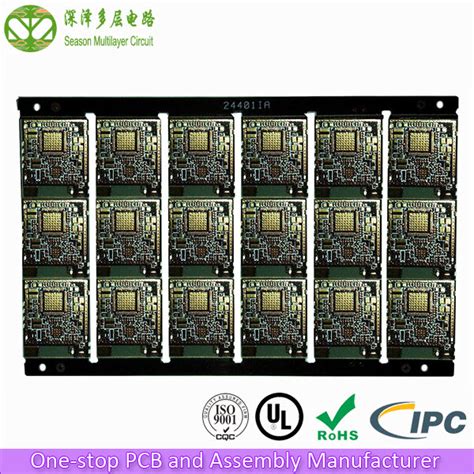
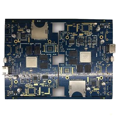
Printed Circuit Boards (PCBs) are the backbone of modern electronics, providing mechanical support and electrical connections for electronic components. One of the most critical steps in PCB manufacturing is the etching process, which removes unwanted copper from the board to create the desired conductive pathways.
This article explores the PCB etching process in detail, covering its principles, methods, materials, advantages, challenges, and best practices. By understanding etching, engineers and hobbyists can improve PCB fabrication quality and efficiency.
1. What is PCB Etching?
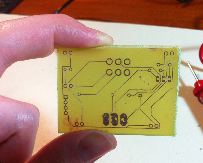
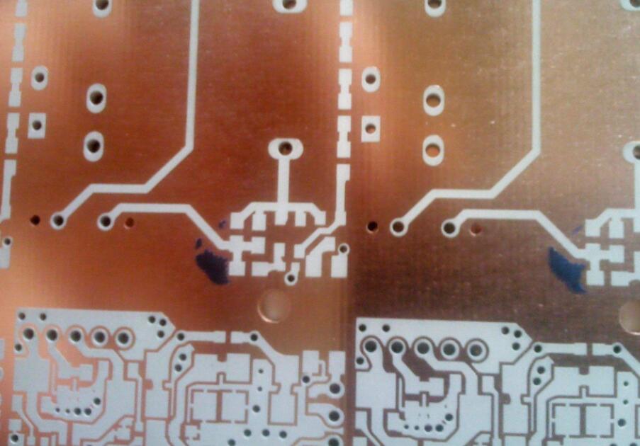
PCB etching is a subtractive manufacturing process where excess copper is chemically removed from a copper-clad laminate, leaving behind the designed circuit traces. The process involves:
- Copper-clad laminate: A non-conductive substrate (usually FR4) coated with a thin layer of copper.
- Etchant: A chemical solution that dissolves unwanted copper.
- Resist layer: A protective mask (usually photoresist or toner transfer) that shields the desired copper traces from the etchant.
The goal is to accurately replicate the circuit design while ensuring minimal undercutting, high precision, and reliable conductivity.
2. Types of PCB Etching Methods
There are several etching techniques, each with its own advantages and limitations:
2.1 Chemical Etching (Wet Etching)
The most common method, chemical etching, involves immersing the PCB in an etchant solution. The main types of chemical etchants are:
a) Ferric Chloride (FeCl₃)
- Pros: Effective, widely available, and works at room temperature.
- Cons: Messy, stains surfaces, and requires careful disposal due to environmental concerns.
- Process:
- Apply a resist (toner, photoresist, or etching pen) to protect the desired traces.
- Submerge the board in FeCl₃ solution (typically 30-40% concentration).
- Agitate to speed up etching (5-20 minutes, depending on copper thickness).
- Rinse with water and remove the resist.
b) Ammonium Persulfate
- Pros: Clear solution, less staining, and faster than ferric chloride.
- Cons: Can decompose over time, requiring fresh solutions.
- Process: Similar to FeCl₃ but often used in industrial settings.
c) Hydrochloric Acid + Hydrogen Peroxide (HCl + H₂O₂)
- Pros: Fast etching, low cost, and easy disposal (neutralize with baking soda).
- Cons: Requires careful handling due to corrosive fumes.
- Process:
- Mix HCl and H₂O₂ in a 2:1 ratio.
- Immerse the PCB and agitate (etching completes in 2-5 minutes).
- Neutralize and rinse thoroughly.
2.2 Electrochemical Etching
- Principle: Uses an electric current to dissolve copper in a conductive solution.
- Pros: More controlled, less chemical waste.
- Cons: Requires specialized equipment.
- Process:
- Place the PCB in an electrolyte bath (e.g., sodium chloride solution).
- Apply a voltage to accelerate copper dissolution.
- The exposed copper is removed selectively.
2.3 Plasma (Dry) Etching
- Principle: Uses ionized gas (plasma) to remove copper.
- Pros: High precision, no liquid chemicals.
- Cons: Expensive, used mainly in high-end PCB manufacturing.
- Process:
- Place the PCB in a vacuum chamber.
- Introduce reactive gases (e.g., CF₄, O₂).
- Plasma ions bombard and remove unwanted copper.
3. Step-by-Step PCB Etching Process
Here’s a detailed walkthrough of a typical chemical etching process:
Step 1: Design the PCB Layout
- Use CAD software (e.g., KiCad, Eagle, Altium) to create the circuit design.
- Print the design on a transparent film (for UV exposure) or glossy paper (for toner transfer).
Step 2: Prepare the Copper-Clad Board
- Clean the board with fine sandpaper or alcohol to remove oxidation.
- Dry thoroughly to ensure proper resist adhesion.
Step 3: Apply the Resist Layer
Option A: Toner Transfer Method (for DIY)
- Print the PCB layout on glossy paper using a laser printer.
- Place the printed side on the copper and apply heat (using an iron or laminator).
- Soak in water to remove the paper, leaving toner on the copper.
Option B: Photoresist Method (for Higher Precision)
- Coat the board with UV-sensitive photoresist.
- Place the transparent film with the design on the board.
- Expose to UV light (the exposed areas harden; unexposed areas remain soluble).
- Develop the board in a sodium hydroxide (NaOH) solution to remove unexposed resist.
Step 4: Etch the PCB
- Immerse the board in the chosen etchant (FeCl₃, HCl+H₂O₂, etc.).
- Agitate gently to ensure even etching.
- Monitor until all unwanted copper dissolves (check by lifting the board periodically).
Step 5: Clean and Inspect
- Rinse with water to stop the etching process.
- Remove the resist using acetone or sandpaper.
- Inspect for defects (e.g., over-etching, incomplete traces).
Step 6: Post-Etching Finishing
- Drill holes for through-hole components.
- Apply solder mask (optional) to protect traces.
- Add silkscreen labels (optional) for component placement.
4. Challenges and Troubleshooting
4.1 Common Issues
- Undercutting: Over-etching causes traces to become thinner than designed.
- Solution: Reduce etching time or use a less aggressive etchant.
- Incomplete Etching: Some copper remains due to insufficient etching time or exhausted etchant.
- Solution: Refresh the etchant or extend etching time.
- Resist Peeling: The protective layer detaches prematurely.
- Solution: Ensure proper cleaning and resist application.
4.2 Environmental and Safety Concerns
- Chemical disposal: Etchants like FeCl₃ are hazardous and must be neutralized before disposal.
- Ventilation: Work in a well-ventilated area to avoid inhaling fumes.
- Protective gear: Use gloves and goggles when handling chemicals.
5. Advantages and Disadvantages of PCB Etching
Advantages
✔ Cost-effective for prototyping and small-scale production.
✔ High precision with photoresist methods.
✔ Compatible with DIY fabrication.
Disadvantages
✖ Chemical waste requires proper disposal.
✖ Limited to simple or moderately complex designs (for DIY methods).
✖ Slower than modern techniques like milling or additive PCB printing.
6. Future Trends in PCB Etching
- Laser Direct Etching: Uses lasers to remove copper without chemicals (eco-friendly).
- Additive Manufacturing: Conductive ink printing reduces waste.
- Improved Eco-Etchants: Development of biodegradable etchants.
Conclusion
The PCB etching process is a fundamental technique in electronics manufacturing, enabling the creation of precise circuit patterns. While chemical etching remains popular for its simplicity and cost-effectiveness, advancements in laser and plasma etching offer cleaner and more efficient alternatives.
By understanding the etching process, engineers can optimize their PCB fabrication for better performance, reliability, and environmental sustainability. Whether for hobbyist projects or industrial production, mastering PCB etching is essential for high-quality electronic design.