PCB Fabrication & Assembly Services: Best Practices
Key Takeaways
Effective PCB fabrication and assembly rely on harmonizing design precision, material selection, and process optimization A critical first step is aligning design files with manufacturing capabilities to minimize errors and delays Design for Manufacturability (DFM) principles, such as maintaining proper trace spacing and avoiding acute angles, directly impact yield rates and long-term reliability
Tip: Conduct DFM checks early in the design phase to identify potential fabrication hurdles, such as impedance mismatches or thermal stress points
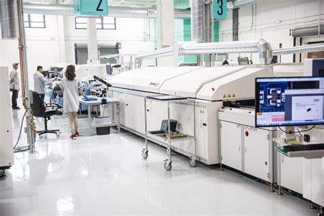
In PCB assembly workflows, selecting the right PCBA (Printed Circuit Board Assembly) partner ensures access to advanced techniques like automated optical inspection (AOI) and X-ray testing These technologies detect solder joint defects or component misalignments that manual inspections might miss For high-density interconnect (HDI) boards, laser drilling and sequential lamination are indispensable for achieving microvia accuracy
Material selection also plays a pivotal role—opting for FR-4 substrates for standard applications or polyimide for flexible circuits balances cost and performance Prioritize suppliers with AS9100 or ISO 9001 certifications to guarantee material traceability and consistency
"A robust quality control framework isn’t optional—it’s the backbone of reliable PCBA outcomes."
Finally, streamline workflows by integrating Enterprise Resource Planning (ERP) systems to track production stages in real time This reduces lead times and ensures seamless coordination between fabrication, assembly, and testing phases By embedding these best practices, manufacturers can achieve faster time-to-market while maintaining stringent quality benchmarks

Optimizing PCB Design for Manufacturing Success
Effective PCB fabrication & assembly begins with design decisions that align with manufacturing capabilities First and foremost, adopting Design for Manufacturing (DFM) principles reduces costly revisions by ensuring layouts meet production tolerances For instance, maintaining adequate trace widths and annular ring sizes prevents soldering defects during pcb assembly, while optimizing component placement minimizes signal interference and thermal hotspots
A critical step involves collaborating with pcba providers early in the design phase to validate material choices and layer stack-ups For example, selecting substrates with appropriate thermal conductivity and dielectric properties ensures reliability in high-frequency or high-temperature applications Advanced CAD tools now integrate real-time DFM checks, flagging issues like insufficient pad spacing or non-standard via sizes before prototyping
Another priority is simplifying panelization strategies to maximize yield Nesting designs efficiently across fabrication panels reduces material waste and lowers per-unit costs—a key consideration for scalable pcb assembly workflows Additionally, incorporating standardized footprint libraries accelerates component sourcing and minimizes errors during automated pick-and-place processes
When preparing files for production, clarity in documentation is non-negotiable Detailed layer-by-layer drawings, coupled with explicit assembly notes for surface finishes or solder mask requirements, prevent misinterpretations For mixed-technology boards requiring both SMT and through-hole components, defining clear keep-out zones ensures compatibility with reflow and wave soldering equipment
By harmonizing design intent with pcba manufacturing realities, engineers create boards that transition seamlessly from prototype to mass production This alignment not only enhances functional performance but also strengthens supply chain resilience—a competitive advantage in today’s fast-paced electronics market
Advanced Assembly Techniques for Reliable PCBs
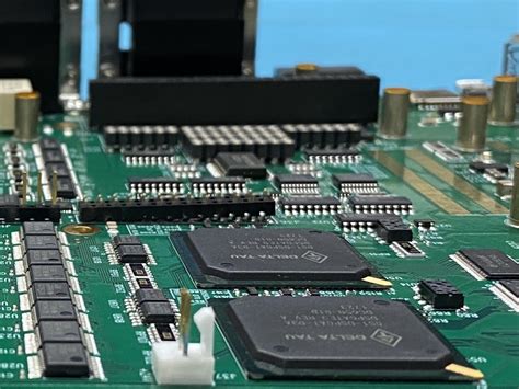
Modern PCB assembly processes demand precision and adaptability to meet increasingly complex design requirements One critical advancement is the integration of surface-mount technology (SMT), which enables the placement of smaller components with higher density, improving both performance and space efficiency Mixed-technology assemblies, combining SMT and through-hole components, are now common in PCBA workflows, particularly for prototypes requiring flexibility
A key innovation lies in automated optical inspection (AOI) systems, which scan solder joints and component alignment at micron-level accuracy Paired with X-ray inspection for hidden connections (e.g., BGAs), these systems reduce defect rates by up to 40% compared to manual checks The table below highlights the impact of advanced inspection methods:
| Technique | Defect Detection Rate | Throughput (Boards/Hour) |
|---|---|---|
| Manual Inspection | 75-85% | 10-15 |
| AOI Systems | 98-99% | 50-70 |
| X-Ray Inspection | 995%+ | 30-50 |
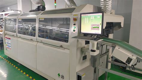
Equally vital is the adoption of nitrogen reflow soldering, which minimizes oxidation during high-temperature processes This technique enhances joint integrity, particularly for fine-pitch ICs and QFN packages For PCBA projects involving harsh environments, conformal coating applications—whether silicone, acrylic, or urethane-based—add an extra layer of protection against moisture and contaminants
To address thermal management challenges, manufacturers now employ 3D solder paste inspection (SPI) to verify deposition volume before component placement This preemptive measure prevents tombstoning and bridging, especially in designs with microvia structures or HDI layouts When combined with predictive maintenance algorithms for pick-and-place machinery, these strategies ensure consistent output even during high-volume production runs
Transitioning seamlessly from design optimization, these advanced techniques form the backbone of modern PCB fabrication and assembly services, setting the stage for rigorous quality control measures in subsequent stages

Implementing Rigorous Quality Control Measures
Effective PCB assembly processes demand meticulous quality control (QC) protocols to ensure the reliability and longevity of electronic devices At the heart of robust QC lies automated optical inspection (AOI), a technology that scans PCBA boards for soldering defects, component misalignment, and trace integrity By integrating AOI at multiple stages—post-solder paste application, component placement, and final assembly—manufacturers can detect anomalies as small as 10µm, reducing rework costs by up to 40%
Another critical component is in-circuit testing (ICT), which verifies electrical performance by simulating real-world operating conditions ICT identifies issues like short circuits, open connections, or incorrect component values, ensuring each PCB assembly meets design specifications For high-density boards, X-ray inspection becomes indispensable, enabling engineers to examine hidden solder joints under ball grid arrays (BGAs) or multilayer configurations
Material consistency plays a pivotal role in QC Implementing traceability systems for solder paste, substrates, and components ensures compliance with industry standards such as IPC-A-610 and ISO 9001 Statistical process control (SPC) tools further enhance reliability by monitoring production variables like reflow oven temperatures or pick-and-place machine accuracy, maintaining process capability indices (Cpk) above 133
To address potential defects in PCBA workflows, many manufacturers adopt failure mode and effects analysis (FMEA) during prototyping This proactive approach identifies risk priorities for critical components, allowing teams to refine assembly parameters before full-scale production Post-assembly, environmental stress testing—including thermal cycling and vibration tests—validates board durability under extreme conditions, a non-negotiable step for aerospace or automotive applications
By combining these strategies with real-time data analytics, PCB fabrication and assembly services achieve defect rates below 50 parts per million (PPM), aligning with Six Sigma principles Continuous feedback loops between QC findings and design teams also foster iterative improvements, ensuring every production batch adheres to evolving industry benchmarks

Cost-Effective Material Selection Strategies
Selecting the right materials for PCB assembly (PCBA) is a critical balancing act between performance, reliability, and budget While high-performance substrates like Rogers or Teflon excel in specialized applications, they often come with significant cost premiums For most commercial and industrial projects, cost-effective material selection begins with prioritizing FR-4 epoxy laminates, which offer a robust combination of electrical insulation, thermal stability, and affordability By aligning material choices with the operational requirements of the end product—such as temperature ranges, signal frequencies, and mechanical stress levels—manufacturers can avoid overspending on unnecessary premium-grade components
A strategic approach involves collaborating with PCBA suppliers early in the design phase to identify substitute materials that meet functional needs without compromising quality For example, using standard copper weights (1 oz/ft² instead of 2 oz/ft²) for non-power-intensive circuits reduces material costs while maintaining conductivity Similarly, opting for lead-free HASL (Hot Air Solder Leveling) over ENIG (Electroless Nickel Immersion Gold) surface finishes can lower expenses in applications where corrosion resistance is sufficient but extreme durability isn’t required
For high-volume production, bulk purchasing agreements for base materials like prepregs and cores further drive down costs Advanced PCB fabrication partners often maintain multi-tiered supplier networks, enabling access to competitively priced, certified materials However, cost-cutting should never sacrifice critical performance metrics—thermal management materials, such as aluminum-clad substrates, remain essential for power electronics to prevent overheating and ensure longevity
Finally, leveraging design-for-manufacturing (DFM) tools helps validate material choices against fabrication constraints, minimizing waste and rework By integrating real-time cost analytics into the selection process, teams can make data-driven decisions that align with both technical specifications and budgetary goals This proactive strategy ensures that PCB assembly projects achieve optimal cost efficiency without compromising the reliability of the final product
Streamlining PCB Fabrication Workflow Processes
Efficient PCB fabrication workflows are critical for reducing lead times while maintaining precision in complex circuit board production A well-optimized process begins with design-to-manufacturing (DFM) validation, where automated tools identify potential fabrication conflicts, such as inadequate trace spacing or drill alignment errors By resolving these issues early, manufacturers minimize costly rework and accelerate time-to-market for PCBA projects
Integrating pcb assembly planning into the fabrication phase further enhances workflow efficiency For instance, synchronizing solder mask application with surface finish selection ensures compatibility with subsequent pick-and-place and reflow soldering stages Advanced factories employ just-in-time (JIT) material procurement strategies, reducing inventory costs without compromising component availability for multilayer pcba builds
Standardized process documentation plays a pivotal role in eliminating bottlenecks Detailed standard operating procedures (SOPs) for laser drilling, copper plating, and AOI (automated optical inspection) create repeatable outcomes across high-mix production runs Real-time monitoring systems track key metrics like etch rate consistency and layer registration accuracy, enabling immediate adjustments during PCB fabrication
The adoption of unified software platforms bridges gaps between design, fabrication, and pcb assembly teams Cloud-based collaboration tools allow concurrent review of Gerber files, Bill of Materials (BOM), and test protocols, ensuring all stakeholders align with evolving project requirements This seamless integration is particularly vital for high-density interconnect (HDI) designs, where micron-level tolerances demand flawless cross-department coordination
By implementing these strategies, manufacturers achieve first-pass yield improvements of up to 30%, while reducing overall pcba production cycles by 15-20% These gains directly translate to enhanced scalability for clients requiring rapid prototyping or large-volume orders without quality trade-offs
Ensuring Signal Integrity Through Layout Best Practices
Achieving optimal signal integrity begins with strategic layout design, a critical phase where electromagnetic interference (EMI) risks and signal degradation can be mitigated In PCB assembly workflows, improper trace routing or component placement often leads to crosstalk, impedance mismatches, or timing errors—issues that compromise performance in high-frequency applications To address these challenges, designers prioritize controlled impedance routing, ensuring trace widths and spacing align with the board’s dielectric properties and target signal speeds
A foundational practice involves separating analog and digital ground planes to prevent noise coupling, particularly in mixed-signal PCBA designs This separation, combined with star-point grounding techniques, minimizes ground loops and stabilizes reference voltages For high-speed signals, differential pair routing becomes essential By maintaining consistent spacing and length matching between pairs, designers preserve signal symmetry, reducing EMI susceptibility
Layer stack-up configuration also plays a pivotal role Placing high-speed signal layers adjacent to solid power or ground planes enhances shielding while minimizing cross-talk Additionally, avoiding sharp angles in trace routing—opting for 45-degree bends or curved traces instead—reduces impedance discontinuities and reflections
In PCB fabrication and assembly, material selection directly impacts signal integrity Low-loss laminates with stable dielectric constants (Dk) are preferred for high-frequency boards, as they minimize signal attenuation Thermal management considerations, such as via placement for heat dissipation, further ensure stable operation under load
Automated design rule checks (DRCs) and simulation tools like SI/PI analysis enable pre-production validation of layout choices By identifying potential bottlenecks early, teams can refine pad geometries, via structures, and decoupling capacitor placement before prototyping This proactive approach not only streamlines PCB assembly but also reduces costly revisions during mass production
Finally, collaboration between design and PCBA teams ensures manufacturability Clear documentation of impedance requirements, solder mask openings, and component orientation prevents misinterpretations during fabrication, preserving the integrity of the final product
Leveraging Automation in PCB Assembly Services
The integration of automation into PCB assembly workflows has revolutionized the production of high-density and complex circuit boards Modern PCBA facilities now deploy robotic pick-and-place systems, automated soldering technologies, and vision-guided inspection tools to achieve micron-level precision These systems eliminate human error while accelerating throughput, particularly for boards requiring thousands of components or ultra-fine pitch placements
A key advantage lies in automated optical inspection (AOI) systems, which perform real-time defect detection during solder paste application, component placement, and post-reflow stages Paired with machine learning algorithms, these systems adapt to evolving design complexities, identifying issues like tombstoning or bridging with 999% accuracy For high-mix production environments, flexible automation enables rapid reconfiguration between different PCB assembly batches, minimizing downtime
Another critical application is in traceability Automated PCBA lines embed unique identifiers (UIDs) at each process stage, creating digital twins of physical boards This data-driven approach simplifies root-cause analysis for quality deviations and ensures compliance with industry standards such as IPC-A-610
While automation requires significant upfront investment, its long-term ROI stems from repeatable quality and scalability Manufacturers leveraging these technologies report 30–50% reductions in assembly defects and 20% faster time-to-market for prototypes To optimize results, engineers must align design files with automated equipment specifications—ensuring component footprints, solder mask clearances, and panelization layouts meet machine tolerances
As PCB assembly evolves, hybrid models combining robotic precision with human expertise are becoming the benchmark This synergy addresses niche challenges like odd-form component placement while maintaining the efficiency gains central to modern PCBA workflows
Adopting Eco-Friendly PCB Production Methods
The electronics manufacturing industry is increasingly prioritizing sustainable practices, with PCB assembly providers integrating eco-conscious strategies into pcba workflows Transitioning to halogen-free laminates and lead-free surface finishes reduces hazardous substance exposure while maintaining board reliability For instance, replacing traditional FR-4 materials with recycled copper-clad laminates can lower carbon footprints by up to 30% without compromising thermal stability
Advanced fabrication techniques like laser direct imaging minimize chemical etchants, reducing wastewater contamination risks Similarly, adopting water-soluble flux in pcb assembly soldering processes eliminates chlorofluorocarbon emissions during cleaning Manufacturers are also optimizing energy consumption through automated panelization algorithms, which decrease material waste by 12–18% in multi-board production runs
Waste management protocols now emphasize closed-loop recycling systems for copper, tin, and precious metals recovered from fabrication byproducts Leading pcba suppliers achieve 95% metal recovery rates through electrolytic refinement, aligning with ISO 14001 environmental standards Transitioning to biodegradable packaging for components and finished boards further complements these efforts, with plant-based anti-static materials gaining traction
Certification programs like IPC-1401 provide frameworks for quantifying sustainability metrics across design, fabrication, and pcb assembly stages By implementing lifecycle assessment tools, engineers can evaluate the ecological impact of substrate choices and assembly methods early in product development This proactive approach not only meets regulatory requirements but also appeals to OEMs seeking LEED-certified supply chains
While initial investments in solar-powered production facilities or zero-discharge plating systems may increase capital costs, long-term operational savings and brand equity gains justify the shift As global regulations tighten, manufacturers that seamlessly integrate eco-friendly practices into pcba services will maintain competitive advantages in markets prioritizing environmental stewardship
Conclusion
The evolution of PCB fabrication and assembly technologies underscores the importance of adopting holistic strategies that bridge design, production, and testing phases By integrating PCB assembly expertise with advanced process automation, manufacturers can achieve unprecedented levels of precision while minimizing human error The synergy between PCBA workflows and rigorous quality assurance protocols ensures that final products meet both performance benchmarks and industry compliance standards
A critical takeaway is the need for cross-functional collaboration during early design stages Proactive engagement between engineers and PCB assembly specialists helps identify potential bottlenecks, such as component placement conflicts or thermal management issues, before they escalate into costly revisions Similarly, leveraging data-driven analytics throughout PCBA processes enables real-time adjustments, optimizing yield rates and material utilization
Sustainability has also emerged as a non-negotiable priority Innovations in lead-free soldering and recyclable substrates demonstrate how eco-conscious practices can coexist with technical excellence Forward-thinking manufacturers are now embedding lifecycle assessments into their PCB fabrication workflows, reducing environmental impact without compromising reliability
Ultimately, success in modern electronics manufacturing hinges on balancing technical innovation with operational pragmatism Whether through adopting AI-driven inspection systems or refining PCBA supply chain logistics, the goal remains consistent: delivering robust, cost-effective circuit boards that power tomorrow’s technologies By prioritizing continuous improvement and stakeholder alignment, businesses can navigate industry challenges while maintaining a competitive edge in an increasingly dynamic market
Frequently Asked Questions
What design considerations impact pcb assembly success?
Implementing design for manufacturability (DFM) principles ensures smooth transitions from prototyping to mass production Key factors include optimizing pad sizes, maintaining proper spacing for automated soldering, and avoiding component overcrowding
How does PCBA differ from standard PCB fabrication?
While fabrication focuses on creating the bare board, PCBA (printed circuit board assembly) involves populating components onto the board Advanced surface-mount technology (SMT) and through-hole assembly techniques are critical for achieving high-density, reliable circuits
What quality checks are vital for pcb assembly reliability?
Rigorous testing protocols like automated optical inspection (AOI) and X-ray verification detect solder joint defects and misalignments Functional testing under simulated operating conditions further validates performance
Can material choices reduce PCBA costs without compromising quality?
Yes, selecting FR-4 alternatives for non-critical layers or using standardized component packages lowers expenses However, high-frequency applications may still require specialized substrates like Rogers material for optimal signal integrity
How do lead times vary between prototyping and bulk pcb assembly?
Prototype services typically deliver in 5-7 days using rapid-turn fabrication, while high-volume orders may require 3-4 weeks due to extended material procurement and multilayer lamination processes
What certifications indicate reliable pcb assembly providers?
Look for ISO 9001 for quality management and IPC-A-610 compliance for assembly workmanship standards Aerospace or medical applications demand additional certifications like AS9100 or ISO 13485
Explore Customized PCB Solutions Today
For tailored pcb assembly strategies that align with your project’s technical and budgetary requirements, please click here to consult our engineering team


