Pcb file
Understanding The Basics Of PCB File Formats
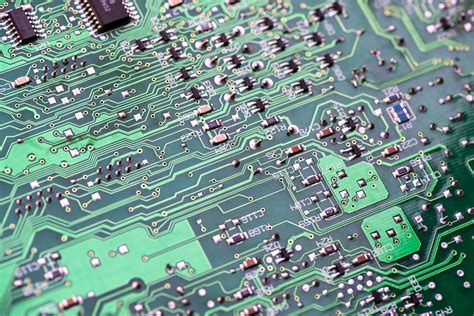
Printed Circuit Boards (PCBs) are the backbone of modern electronic devices, serving as the foundation upon which electronic components are mounted and interconnected. The design and manufacturing of PCBs involve various stages, each requiring precise and detailed information. This information is encapsulated in PCB file formats, which are essential for ensuring that the final product meets the desired specifications. Understanding the basics of PCB file formats is crucial for anyone involved in electronics design and manufacturing.
To begin with, PCB file formats are digital representations of the physical and electrical characteristics of a PCB.
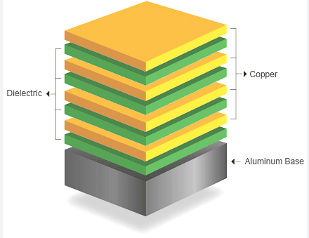
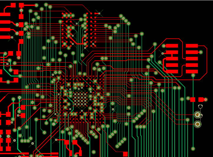
These files contain detailed information about the layout, components, and connections of the board. The most commonly used PCB file format is the Gerber file, which has become the industry standard. Gerber files are vector image files that describe the copper layers, solder mask, legend, and other essential features of a PCB. They are used by PCB manufacturers to create the physical board from the digital design.
In addition to Gerber files, there are several other file formats that play a critical role in the PCB design process.
For instance, the Excellon file format is used to provide information about the drilling process, including the size and location of holes. This format is essential for ensuring that the vias and through-holes are accurately placed and sized. Another important file format is the Bill of Materials (BOM), which lists all the components required for the PCB assembly. The BOM includes details such as part numbers, quantities, and descriptions, enabling manufacturers to source and assemble the components correctly.
Transitioning from the design phase to the manufacturing phase, it is important to consider the role of design software in generating these file formats.
PCB design software, such as Altium Designer, Eagle, and KiCad, allows designers to create and export the necessary files in the appropriate formats. These software tools provide a user-friendly interface for designing the PCB layout, placing components, and routing connections. Once the design is complete, the software can generate the Gerber, Excellon, and BOM files, among others, which can then be sent to the manufacturer.
Moreover, it is essential to understand the importance of file verification and validation in the PCB design process.
Before sending the files to the manufacturer, designers must ensure that the files are accurate and free of errors. This involves checking for issues such as missing or overlapping traces, incorrect drill sizes, and incomplete BOM entries. Many PCB design software tools include built-in verification features that can help identify and correct these issues. Additionally, third-party verification tools are available to provide an extra layer of assurance.
Furthermore, the evolution of PCB file formats has led to the development of more advanced and integrated formats.
One such example is the ODB++ format, which combines multiple files into a single, comprehensive file. ODB++ includes information about the PCB layout, components, drill data, and more, streamlining the manufacturing process and reducing the risk of errors. This format is gaining popularity due to its ability to simplify data exchange between designers and manufacturers.
In conclusion, understanding the basics of PCB file formats is fundamental for successful PCB design and manufacturing. From Gerber files to BOMs, each format plays a vital role in conveying the necessary information to create a functional and reliable PCB. By leveraging design software and verification tools, designers can ensure that their files are accurate and ready for production. As technology continues to advance, the development of integrated file formats like ODB++ promises to further enhance the efficiency and reliability of the PCB manufacturing process.
How To Convert PCB Files Between Different Software
Printed Circuit Board (PCB) design is a critical aspect of modern electronics, and the ability to convert PCB files between different software platforms is essential for engineers and designers. This process can be complex due to the variety of file formats and the specific features of each software. However, understanding the fundamental steps and tools available can simplify the conversion process, ensuring seamless transitions and maintaining the integrity of the design.
To begin with, it is important to recognize the common file formats used in PCB design software.
Some of the most prevalent formats include Gerber files, which are standard for manufacturing, and proprietary formats like Eagle’s .brd, Altium Designer’s .PcbDoc, and KiCad’s .kicad_pcb. Each of these formats has unique characteristics and is tailored to the specific capabilities of the respective software. Therefore, converting between these formats requires careful attention to detail to avoid data loss or design errors.
One of the primary methods for converting PCB files is using intermediary formats.
Gerber files, for instance, serve as a universal language for PCB manufacturing and can be generated by most PCB design software. By exporting the design to Gerber files, one can then import these files into another software platform. This method, while effective, may not retain all the design elements such as component placement and netlist information, which are crucial for further editing. Consequently, additional steps may be necessary to re-establish these elements in the new software.
Another approach involves using dedicated conversion tools or scripts.
Several software platforms offer built-in or third-party tools designed to facilitate file conversion. For example, Altium Designer provides importers for Eagle and KiCad files, allowing users to open and edit these files directly within Altium. Similarly, KiCad includes tools to import Eagle files, although the process may require some manual adjustments. These tools can significantly streamline the conversion process, but it is essential to verify the accuracy of the converted design thoroughly.
In addition to built-in tools, there are standalone conversion utilities available.
Programs like PCB Converter and online services such as EasyEDA offer capabilities to convert between various PCB file formats. These utilities can be particularly useful when dealing with less common formats or when the native software lacks robust import/export features. However, it is crucial to ensure that these tools are up-to-date and compatible with the latest versions of the software being used.
Moreover, it is advisable to maintain a systematic approach when converting PCB files.
Start by creating a backup of the original design to prevent any loss of data. Next, export the design to an intermediary format if necessary, and use the appropriate conversion tool or script. After importing the design into the new software, meticulously review the layout, component placement, and netlist to ensure that all elements have been accurately transferred. This step is vital to identify and rectify any discrepancies that may have arisen during the conversion process.
In conclusion, converting PCB files between different software platforms is a nuanced task that requires a thorough understanding of the file formats and available tools. By leveraging intermediary formats, utilizing dedicated conversion tools, and adhering to a systematic approach, designers can effectively manage this process. Ensuring the accuracy and integrity of the converted design is paramount, as it directly impacts the functionality and manufacturability of the final product. With careful attention to detail and the right resources, seamless conversion of PCB files can be achieved, facilitating collaboration and innovation in the field of electronics design.
Common Issues And Solutions In PCB File Design
Printed Circuit Board (PCB) file design is a critical aspect of modern electronics, serving as the backbone for virtually all electronic devices. However, the process of designing PCB files is fraught with potential issues that can compromise the functionality, reliability, and manufacturability of the final product. Understanding these common issues and their solutions is essential for engineers and designers aiming to produce high-quality PCBs.
One prevalent issue in PCB file design is improper component placement.
Components that are not strategically placed can lead to signal integrity problems, increased electromagnetic interference (EMI), and difficulties in heat dissipation. To mitigate these issues, designers should follow best practices such as placing high-speed components close to each other to minimize signal path lengths and grouping components with similar functions together. Additionally, thermal management can be improved by placing heat-generating components in areas with adequate airflow or near heat sinks.
Another common problem is inadequate trace width and spacing.
Traces that are too narrow can lead to increased resistance and potential overheating, while insufficient spacing between traces can result in short circuits. To address this, designers should adhere to the design rules provided by PCB manufacturing standards, such as IPC-2221, which specify minimum trace widths and spacing based on current-carrying requirements and voltage levels. Utilizing design rule checks (DRCs) within PCB design software can also help identify and rectify these issues early in the design process.
Signal integrity issues, such as crosstalk and reflection, are also frequent challenges in PCB file design.
Crosstalk occurs when a signal in one trace induces an unwanted signal in an adjacent trace, while reflection happens when a signal encounters impedance mismatches along its path. To combat these problems, designers can use techniques such as controlled impedance routing, differential pair routing, and proper termination of signal lines. Additionally, maintaining a consistent ground plane and using decoupling capacitors can help stabilize voltage levels and reduce noise.
Power distribution is another critical aspect that can present challenges.
Inadequate power distribution can lead to voltage drops and insufficient power delivery to components, affecting the overall performance of the PCB. To ensure robust power distribution, designers should use power planes and wide traces for power and ground connections. Implementing a star topology for power distribution, where each component is connected directly to a central power source, can also help maintain consistent voltage levels across the board.
Thermal management is a significant concern, especially in high-power applications.
Poor thermal management can lead to overheating and potential failure of components. To address this, designers can use thermal vias to transfer heat from the top layer to inner or bottom layers, employ heat sinks, and ensure adequate spacing between heat-generating components. Additionally, using materials with high thermal conductivity for the PCB substrate can help dissipate heat more effectively.
Finally, manufacturability issues can arise if the PCB design is not optimized for the fabrication process.
This includes problems such as insufficient solder mask clearance, non-standard hole sizes, and complex board shapes that are difficult to produce. To avoid these issues, designers should collaborate closely with PCB manufacturers during the design phase and follow design for manufacturability (DFM) guidelines. This collaboration ensures that the design is compatible with the manufacturer’s capabilities and reduces the likelihood of production delays or defects.
In conclusion, while PCB file design is a complex and challenging process, understanding and addressing common issues such as component placement, trace width and spacing, signal integrity, power distribution, thermal management, and manufacturability can significantly enhance the quality and reliability of the final product. By adhering to best practices and leveraging advanced design tools, engineers and designers can overcome these challenges and create robust, high-performance PCBs.
Best Practices For Organizing And Managing PCB Files
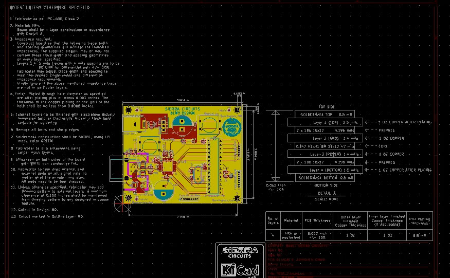
Printed Circuit Board (PCB) files are essential components in the design and manufacturing of electronic devices. Proper organization and management of these files are crucial for ensuring efficient workflow, minimizing errors, and facilitating collaboration among team members. To achieve these objectives, several best practices should be adhered to, starting with the establishment of a clear and consistent file naming convention. This practice helps in quickly identifying the purpose and version of each file, thereby reducing confusion and the risk of using outdated or incorrect files.
In addition to naming conventions, it is important to maintain a well-structured directory system.
Organizing files into specific folders based on their function, such as design files, manufacturing files, and documentation, can significantly enhance accessibility. Within these folders, further categorization by project or component type can streamline the retrieval process. This hierarchical structure not only aids in locating files swiftly but also ensures that all team members can easily navigate the file system.
Version control is another critical aspect of managing PCB files.
Utilizing version control software allows for tracking changes, reverting to previous versions if necessary, and maintaining a history of modifications. This is particularly beneficial in collaborative environments where multiple individuals may be working on the same project. By implementing version control, teams can avoid the pitfalls of overwriting each other’s work and ensure that the most current and accurate files are always in use.
Moreover, regular backups are indispensable for safeguarding PCB files against data loss.
Establishing a routine backup schedule, whether daily, weekly, or after significant changes, can prevent the loss of valuable work due to hardware failures, software issues, or human error. Storing backups in multiple locations, such as on local drives and cloud storage, provides an additional layer of security.
Documentation plays a pivotal role in the effective management of PCB files.
Comprehensive documentation should accompany each project, detailing the design process, component specifications, and any modifications made. This not only aids in the understanding and replication of the design but also serves as a reference for troubleshooting and future updates. Including metadata within the files themselves, such as author information, creation date, and version number, further enhances traceability and accountability.
Furthermore, standardizing the design process can lead to more consistent and reliable outcomes.
Adopting industry-standard design rules and guidelines ensures that PCB files are compatible with manufacturing processes and meet quality standards. Regularly reviewing and updating these standards in response to technological advancements and feedback can help maintain their relevance and effectiveness.
Effective communication among team members is also vital for the successful organization and management of PCB files. Regular meetings and updates can help keep everyone informed about the project’s progress and any changes to the file management system. Utilizing collaborative tools and platforms can facilitate real-time sharing and editing of files, thereby enhancing teamwork and productivity.
Lastly, continuous education and training on best practices for PCB file management can empower team members to adhere to established protocols and contribute to the overall efficiency of the workflow. Keeping abreast of new tools, techniques, and industry trends can provide valuable insights and improvements to existing practices.
In conclusion, organizing and managing PCB files effectively requires a combination of clear naming conventions, structured directories, version control, regular backups, thorough documentation, standardized design processes, effective communication, and ongoing education. By implementing these best practices, teams can ensure the integrity, accessibility, and reliability of their PCB files, ultimately leading to more successful and efficient project outcomes.