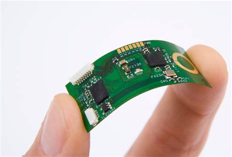
PCB film product manufacturing process
The manufacturing process of PCB (printed circuit board) using resin film products has unique technical characteristics and advantages, which is worth in-depth discussion. Resin film is a functional material, usually made of polyimide (PI), polyester (PET) or other synthetic resins. The excellent properties of these materials make PCB widely used in modern electronic devices.
First, the heat resistance and chemical stability of resin film make it perform well in high temperature and harsh environments. This is especially important for high-frequency and high-power circuit designs, which often face the challenges of extreme temperatures and chemical corrosion. The thermal stability of resin film not only ensures the reliability of the circuit, but also effectively extends the service life of the equipment. Secondly, the insulation performance of resin film is excellent, which can effectively block current and reduce electromagnetic interference. As electronic products develop towards smaller and higher density, high-quality insulating materials are particularly important. The high dielectric strength of resin film provides ideal insulation support for complex circuits, making the design and manufacture of multi-layer PCBs possible. In addition, the processing flexibility of resin film is also a major advantage. By adjusting the resin formula and processing conditions, manufacturers can achieve resin films of different thicknesses, colors and textures to meet the diverse needs of customers. For example, in some high-end applications, light-transmitting resin films can be used to manufacture LED displays, while wear-resistant resin films are suitable for manufacturing touch panels. These innovations have led to the continuous expansion of PCB application areas.
In terms of manufacturing process, the use of resin films simplifies the traditional PCB production process. Through precise coating and curing processes, resin films can achieve high-quality products at a lower cost. In addition, resin films generate less waste during the production process, which helps companies improve their environmental image and conforms to the trend of sustainable development in modern manufacturing.
In general, the manufacturing process of resin film products for PCBs not only has excellent technical characteristics, but also meets the market’s multiple requirements for high performance, low cost and environmental protection. This makes resin films play an indispensable role in the electronics industry, promoting technological progress and product innovation.
(1) Manufacturing process of resin film products
The production of resin film products with support bodies is usually carried out on a high-precision coating machine. First, the liquid resin is evenly coated on the surface of the carrier, and then a resin composition layer is formed by drying. Next, after cutting and winding, a semi-cured resin film is obtained.
Given the differences in the composition of the resin film, the subsequent processing techniques are also different. Some patents point out that the resin film dried by the coater may need to be further heat-cured in a heating oven to ensure that the performance of the material meets the expected standards. The figure below shows the manufacturing process of the resin film for PCB disclosed in the patent of Hitachi Chemical Co., Ltd., which is particularly suitable for producing a two-layer resin film product.
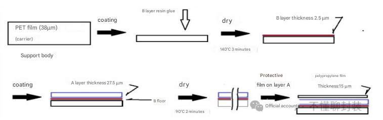
The method for manufacturing the resin film is not limited to a single form. Usually, the resin layer is obtained by coating the resin composition on the supporting substrate and drying it. A variety of coating equipment can be used, such as a kiss coater, a roller coater or a dot coater. After the resin composition is applied to the support, it needs to be dried in a heating drying oven. For example, it is preferably dried at a temperature of 70 to 200°C for 1 to 30 minutes (more preferably 3 to 15 minutes) to make the resin composition reach a semi-cured state and form a resin film. The thickness of the resin film can be set between 3 and 150 μm, and the specific preferred value should be adjusted according to the required printed circuit board characteristics. When setting the thickness of the resin film, it is necessary to take into account the two main principles of achieving thinness and excellent high-frequency characteristics, so as to ensure the reliability and effectiveness of the product in high-performance applications.
(2) Product structure characteristics of resin film
At present, resin film products with support bodies are mainly divided into two types of structural forms: single-layer film structure resin products (referred to as single-layer resin film) and composite film structure resin film (referred to as composite resin film). Among them, composite resin film is mainly a two-layer resin film, which is widely used in high-performance printed circuit boards (PCBs) and other fields. These two structures have their own characteristics and meet different application needs and performance requirements.
The advantage of single-layer resin film structure products for PCB is that they are relatively easy to develop and produce, and they excel in thickness precision control and thinning. However, the manufacturing technology of two-layer resin film products is at a higher level. This structure is composed of two layers of resin, which can reasonably share the functions and create conditions for reducing material costs. It represents the new trend of the current development of resin films in terms of varieties and technologies.
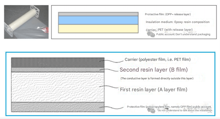
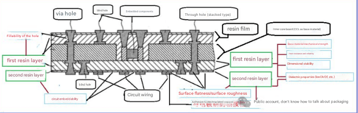
From the perspective of “function sharing”, you can refer to the two-layer resin film structure diagram shown in the Hitachi Chemical patent in the above figure to deepen your understanding. The first resin layer (referred to as “A layer” in some Hitachi Chemical patents) is mainly responsible for ensuring the following key properties of the substrate: the strength of the entire film substrate (with elastic modulus as the main evaluation index), heat resistance reliability (with glass transition temperature Tg and cycle endurance as evaluation criteria), dielectric properties (with dielectric constant Dk, dielectric loss Df and transmission loss as references), dimensional stability (with thermal expansion coefficient CTE as evaluation basis), and in the case of through holes and blind holes, ensuring sufficient embedding of the resin in the hole (called “hole embedding property”).
The second resin layer (referred to as “B layer” in some Hitachi Chemical patents) directly forms a circuit layer on its surface, mainly through the chemical plating process to form a conductive layer. This layer mainly ensures the superiority of fine circuit processing performance. In order to achieve excellent fine circuit processing performance, the film substrate needs to have good surface flatness, appropriate surface roughness, good adhesion to electroplated copper, and excellent circuit embedding performance (also known as “circuit embedding property” or “circuit embedding property”). Obviously, the quality of these properties is closely related to the quality of the second resin layer. The second resin layer also needs to share the excellent dielectric properties with the first layer (layer A), especially in reducing dielectric loss (Df), to ensure the high performance of the overall film substrate.
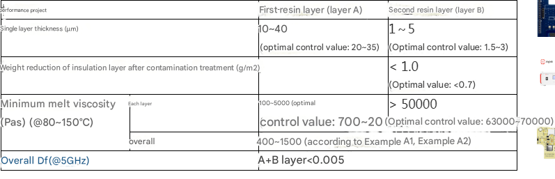
Since the first and second resin layers (layer A and layer B) have different focuses on “functional contribution”, that is, there is a certain “division of labor”, they also have different performance index control. Detailed information about this difference is disclosed in the Japanese patent on the development of a two-layer resin film (for high-frequency circuits and multi-layer PCBs using the SAP method to form a conductive layer). The relevant content is sorted and listed in the following table for reference and example.