PCB Finger Connector: A Comprehensive Overview
Introduction
Printed Circuit Board (PCB) finger connectors, also known as edge connectors, are critical components in the electronics industry. They provide a reliable and efficient means of connecting PCBs to other circuit boards, devices, or systems. These connectors are widely used in various applications, ranging from consumer electronics to industrial machinery, due to their simplicity, durability, and cost-effectiveness. This article delves into the design, functionality, types, applications, and future trends of PCB finger connectors, providing a comprehensive understanding of their role in modern electronics.
1. What is a PCB Finger Connector?
A PCB finger connector is a type of electrical connector that is directly integrated into the edge of a PCB. It consists of a series of exposed conductive pads or “fingers” that are plated with a conductive material, typically gold, tin, or nickel. These fingers are designed to mate with a corresponding connector, often referred to as a card-edge connector, which has spring-loaded contacts that press against the fingers to establish an electrical connection.
The primary advantage of PCB finger connectors is their ability to provide a direct connection between the PCB and another device without the need for additional cables or connectors. This reduces the overall complexity and cost of the system while improving reliability.
2. Design and Construction
The design of a PCB finger connector is relatively straightforward but requires careful consideration of several factors to ensure optimal performance. The key elements of a PCB finger connector include:
- Conductive Pads (Fingers): These are the exposed metal traces on the edge of the PCB that serve as the contact points. The fingers are typically plated with a conductive material to enhance conductivity and prevent oxidation. Gold plating is commonly used for high-reliability applications due to its excellent conductivity and resistance to corrosion.
- PCB Edge: The edge of the PCB where the fingers are located must be precisely machined to ensure a proper fit with the mating connector. The edge is often beveled to facilitate insertion and removal.
- Pitch and Spacing: The pitch refers to the distance between the centers of adjacent fingers, while the spacing is the gap between them. These dimensions must be carefully controlled to ensure compatibility with the mating connector and to prevent short circuits.
- Thickness: The thickness of the PCB and the fingers must be consistent to ensure a reliable connection. Variations in thickness can lead to poor contact and increased resistance.
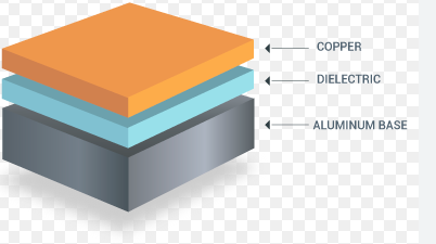
- Material: The base material of the PCB, typically FR-4, must be chosen based on the application’s requirements, including thermal and mechanical properties.

3. Types of PCB Finger Connectors
PCB finger connectors can be categorized based on several criteria, including the number of contacts, the type of plating, and the application. Some common types include:
- Single-Row vs. Double-Row Connectors: Single-row connectors have a single row of fingers along one edge of the PCB, while double-row connectors have two rows, one on each side of the PCB. Double-row connectors offer higher contact density and are used in applications requiring more connections.
- Gold-Plated vs. Tin-Plated Connectors: Gold-plated connectors offer superior conductivity and corrosion resistance, making them ideal for high-reliability applications. Tin-plated connectors are more cost-effective and are suitable for less demanding applications.
- Standard vs. High-Density Connectors: Standard connectors have a larger pitch and are easier to manufacture and assemble. High-density connectors have a smaller pitch and are used in applications where space is at a premium.
- Right-Angle vs. Vertical Connectors: Right-angle connectors are designed to mate with a connector that is perpendicular to the PCB, while vertical connectors mate with a connector that is parallel to the PCB. The choice depends on the system’s mechanical design.
4. Applications of PCB Finger Connectors
PCB finger connectors are used in a wide range of applications across various industries. Some of the most common applications include:
- Consumer Electronics: PCB finger connectors are widely used in consumer electronics, such as smartphones, tablets, and laptops, where they provide a reliable connection between the main PCB and peripheral components, such as displays, cameras, and batteries.
- Industrial Equipment: In industrial machinery, PCB finger connectors are used to connect control boards, sensors, and actuators. Their durability and reliability make them suitable for harsh environments.
- Automotive Electronics: In the automotive industry, PCB finger connectors are used in various electronic systems, including engine control units, infotainment systems, and advanced driver-assistance systems (ADAS). They must withstand high temperatures, vibrations, and exposure to chemicals.
- Medical Devices: Medical devices, such as imaging equipment, patient monitors, and diagnostic tools, often use PCB finger connectors due to their reliability and compact size.
- Aerospace and Defense: In aerospace and defense applications, PCB finger connectors are used in avionics, communication systems, and radar equipment. They must meet stringent requirements for reliability, durability, and performance in extreme conditions.
5. Advantages of PCB Finger Connectors
PCB finger connectors offer several advantages over other types of connectors, including:
- Simplicity: PCB finger connectors are simple in design and do not require additional components, such as cables or housings, reducing the overall complexity of the system.
- Cost-Effectiveness: The integration of the connector directly into the PCB reduces material and assembly costs, making PCB finger connectors a cost-effective solution.
- Reliability: The direct connection between the PCB and the mating connector minimizes the number of contact points, reducing the risk of connection failures.
- Space Efficiency: PCB finger connectors are compact and do not require additional space on the PCB, making them ideal for applications where space is limited.
- Durability: PCB finger connectors are designed to withstand repeated insertion and removal, making them suitable for applications requiring frequent maintenance or replacement.
6. Challenges and Considerations
Despite their many advantages, PCB finger connectors also present some challenges that must be addressed during design and implementation:
- Wear and Tear: Repeated insertion and removal of the connector can lead to wear on the fingers, potentially affecting the quality of the connection over time. Proper plating and material selection can mitigate this issue.
- Alignment: Precise alignment between the PCB and the mating connector is critical to ensure a reliable connection. Misalignment can lead to poor contact and increased resistance.
- Environmental Factors: PCB finger connectors must be designed to withstand environmental factors, such as temperature fluctuations, humidity, and exposure to chemicals, depending on the application.
- Signal Integrity: In high-speed applications, the design of the PCB finger connector must consider signal integrity, including impedance matching and crosstalk, to ensure reliable data transmission.
7. Future Trends
As the electronics industry continues to evolve, PCB finger connectors are expected to undergo several advancements to meet the demands of emerging technologies:
- Miniaturization: The trend toward smaller and more compact devices will drive the development of even smaller PCB finger connectors with higher contact densities.
- High-Speed Data Transmission: With the increasing demand for high-speed data transmission, PCB finger connectors will need to support higher frequencies and maintain signal integrity in high-speed applications.
- Enhanced Durability: Future PCB finger connectors will likely incorporate advanced materials and coatings to enhance durability and reliability, particularly in harsh environments.
- Integration with Advanced Manufacturing Techniques: The integration of PCB finger connectors with advanced manufacturing techniques, such as 3D printing and flexible PCBs, will open up new possibilities for innovative designs and applications.
Conclusion
PCB finger connectors are indispensable components in modern electronics, offering a simple, cost-effective, and reliable means of connecting PCBs to other devices. Their versatility and durability make them suitable for a wide range of applications, from consumer electronics to aerospace and defense. As technology continues to advance, PCB finger connectors will evolve to meet the demands of emerging applications, ensuring their continued relevance in the electronics industry. By understanding the design, functionality, and challenges associated with PCB finger connectors, engineers can make informed decisions when selecting and implementing these connectors in their designs.