PCB Footprint Design: A Comprehensive Guide for Engineers
Introduction to PCB Footprints
Printed Circuit Board (PCB) footprints, also known as land patterns, are essential elements in electronic design that define the physical interface between a component and the PCB. A footprint specifies the copper pads, solder mask openings, silkscreen outlines, and other features necessary to physically and electrically connect a component to a circuit board. Proper footprint design is critical for successful PCB manufacturing, assembly, and long-term reliability.
In modern electronics, where components continue to shrink in size while increasing in complexity, footprint design has become both more challenging and more important. A well-designed footprint ensures proper solder joint formation, minimizes assembly defects, and contributes to the overall reliability of the electronic product. Conversely, poor footprint design can lead to manufacturing difficulties, assembly defects, and field failures.
Fundamentals of PCB Footprint Design
Basic Elements of a Footprint
A complete PCB footprint consists of several key elements:
- Copper Pads: The conductive areas where component leads or terminals make electrical and mechanical connections
- Solder Mask Openings: Windows in the solder mask that expose the copper pads for soldering
- Silkscreen Outline: Visual representation of the component on the PCB
- Assembly Outline: Reference for component placement during assembly
- Courtyard Area: Keep-out zone around the component to prevent interference with adjacent components
- Reference Designator: Unique identifier for the component (e.g., R1, C5, U3)
- Polarity Markings: Indicators for proper component orientation
Footprint Standards and Guidelines
Several industry standards provide guidelines for footprint design:
- IPC-7351: The most widely used standard for surface mount design and land pattern standards
- IPC-SM-782: Covers surface mount design and land pattern standards (now largely superseded by IPC-7351)
- JEDEC Standards: Provide package dimensions and suggested footprints for many semiconductor packages
- Manufacturer Recommendations: Component datasheets often include suggested land patterns
The IPC-7351 standard introduces three density levels for footprints:
- Most (Maximum) Land Protrusion: Provides the most robust solder joints but requires more board space
- Nominal (Median) Land Protrusion: Balanced approach between robustness and space savings
- Least (Minimum) Land Protrusion: Minimizes board space but may reduce solder joint reliability
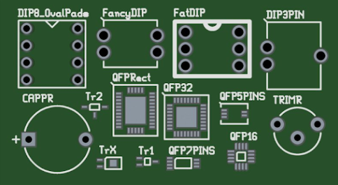
Surface Mount Technology (SMT) Footprints
Common SMT Package Types
- Resistors and Capacitors:
- 0201, 0402, 0603, 0805, 1206, etc.
- Metric equivalents: 008004, 01005, 0201, 0402, 0603, etc.
- Integrated Circuits:
- Small Outline Integrated Circuit (SOIC)
- Thin Small Outline Package (TSOP)
- Quad Flat Package (QFP)
- Quad Flat No-leads (QFN)
- Ball Grid Array (BGA)
- Wafer-Level Chip Scale Package (WLCSP)
- Discrete Semiconductors:
- SOD (Small Outline Diode)
- SOT (Small Outline Transistor)
Design Considerations for SMT Footprints
- Pad Geometry: Must accommodate component termination while allowing proper solder fillet formation
- Solder Mask Design: Typically 50-100μm larger than the pad on each side
- Paste Mask: Often slightly smaller than the pad (80-90%) to prevent solder bridging
- Thermal Relief: Important for components that may require rework or heat dissipation
- Component Orientation: Consistent orientation improves assembly efficiency
Through-Hole Technology (THT) Footprints
Common THT Package Types
- Axial Leads: Used for resistors, diodes, and capacitors
- Radial Leads: Common for electrolytic capacitors and some connectors
- Dual In-line Package (DIP): Traditional IC packaging
- Pin Headers: For connectors and board-to-board connections
Design Considerations for THT Footprints
- Hole Size: Typically 0.2-0.3mm larger than lead diameter for hand soldering, less for wave soldering
- Pad Size: Should be at least 0.5mm larger than the hole diameter
- Annular Ring: Copper around the hole should be sufficient to ensure reliability (typically ≥0.15mm)
- Thermal Relief: Important for multilayer boards to prevent heat sinking during soldering
Advanced Footprint Design Considerations
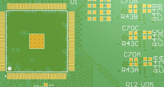
High-Density Interconnect (HDI) Footprints
As components continue to shrink, HDI footprints present special challenges:
- Micro-BGA: Packages with ball pitches of 0.4mm or less
- Fine-Pitch QFP: Packages with lead pitches of 0.5mm or less
- Via-in-Pad: Placing vios directly in pads to save space
- Buried and Blind Vios: Used to route out from dense packages
High-Power Components
Footprints for power components require special considerations:
- Thermal Pads: Large copper areas for heat dissipation
- Thermal Vios: To conduct heat to inner or opposite board layers
- Current Capacity: Pads must handle the required current without excessive heating
RF and High-Speed Digital Components
For high-frequency applications:
- Controlled Impedance: Pad geometries affect transmission line properties
- Grounding: Proper grounding schemes are critical
- Signal Integrity: Pad and via design affects signal quality
Footprint Creation Process
Step-by-Step Footprint Development
- Gather Component Information:
- Manufacturer’s datasheet
- IPC standards
- Package dimensions
- Determine Design Rules:
- PCB manufacturer capabilities
- Assembly process requirements
- Reliability requirements
- Create Geometry:
- Draw pads according to calculated dimensions
- Add solder mask and paste mask layers
- Create silkscreen and assembly outlines
- Add Reference Information:
- Reference designator
- Polarity markings
- Pin 1 indicator
- Verify Dimensions:
- Check against component dimensions
- Verify clearances
- Confirm courtyard areas
Verification and Validation
- Design Rule Check (DRC): Automated checks within the PCB design software
- 3D Modeling: Visualization of the component on the footprint
- Assembly Simulation: Checking for component-to-component interference
- Prototype Testing: Physical verification with actual components
Common Footprint Design Mistakes and How to Avoid Them
- Incorrect Pad Dimensions:
- Problem: Leads to poor solder joints or tombstoning
- Solution: Always verify against component and IPC standards
- Insufficient Solder Mask Clearance:
- Problem: Causes solder bridging or insufficient solder
- Solution: Follow manufacturer recommendations for mask expansion
- Missing or Incorrect Polarity Markings:
- Problem: Leads to assembly errors
- Solution: Implement consistent polarity marking scheme
- Inadequate Courtyard Clearance:
- Problem: Components too close together
- Solution: Include proper keep-out areas in footprint design
- Incorrect Pin 1 Designation:
- Problem: Components placed backwards
- Solution: Clearly mark pin 1 and verify against datasheet
Best Practices for PCB Footprint Design
- Use Standardized Libraries: Maintain consistent, verified footprint libraries
- Follow IPC Standards: Use IPC-7351 as the basis for designs
- Document Assumptions: Record any deviations from standards
- Consider Manufacturing Processes: Design for your specific assembly method
- Implement Version Control: Track changes to footprint libraries
- Collaborate with Manufacturers: Get feedback on your footprint designs
- Regularly Update Libraries: Incorporate new components and design knowledge
Future Trends in Footprint Design
- Smaller Components: Continued miniaturization driving finer pitch footprints
- 3D Packaging: Footprints accommodating stacked die and complex packages
- Embedded Components: Footprints for components placed within PCB layers
- Advanced Materials: Designs accommodating flexible and stretchable electronics
- AI-Assisted Design: Machine learning tools to optimize footprint geometries
- Sustainability Considerations: Designs facilitating recycling and repair
Conclusion
PCB footprint design is a critical aspect of electronic product development that bridges the gap between component packaging and PCB manufacturing. A well-designed footprint ensures reliable electrical connections, facilitates efficient assembly, and contributes to the long-term reliability of the electronic product. By understanding the fundamentals of footprint design, following industry standards, and implementing best practices, engineers can create robust footprints that meet the demands of modern electronics.
As electronic components continue to evolve in size, complexity, and performance requirements, footprint design will remain a challenging and essential skill for PCB designers. Staying current with industry standards, manufacturing capabilities, and emerging technologies will be key to successful footprint design in the years to come.
Remember that while automated tools and library components can be helpful, nothing replaces careful verification and validation of footprints against component specifications and manufacturing requirements. Investing time in proper footprint design pays dividends throughout the product lifecycle, from prototyping to mass production to field performance.