PCB/FPC electrical testing technology analysis
1.Electrical testing
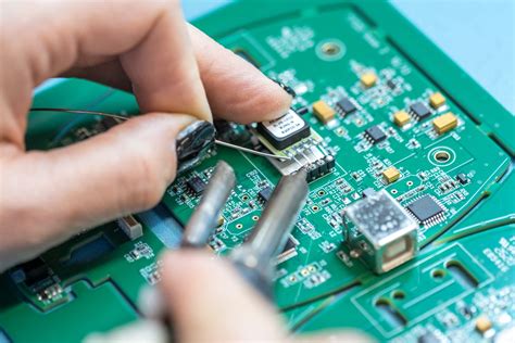
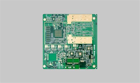
During the production process of PCB boards, it is inevitable that short circuits, open circuits and leakage defects will occur due to external factors. In addition, PCBs are constantly evolving towards high density, fine pitch and multi-layer. If the bad boards are not screened out in time and allowed to flow into the process, it will inevitably cause more cost waste. Therefore, in addition to improving process control, improving testing technology can also provide PCB manufacturers with solutions to reduce scrap rates and increase product yields.
In the production process of electronic products, the cost loss caused by defects has different degrees at each stage. The earlier the discovery, the lower the cost of remediation. “The Rule of 10”s” is a rule that is often used to evaluate the remediation cost of PCBs when defects are found at different stages of the process. For example, after the blank board is made, if the circuit break in the board can be detected in real time, usually only the line needs to be repaired to improve the defect, or at most a blank board will be lost; but if the circuit break is not detected, the board will be shipped to the downstream assembly industry to complete the parts installation, and it will also be remelted by furnace tin and IR. However, if the circuit break is detected at this time, the general downstream assembly industry will ask the blank board manufacturing company to compensate for the parts cost, rework fee, inspection fee, etc. If it is more unfortunate, the defective board is still not discovered during the test of the assembly industry, and enters the overall system finished product, such as computers, mobile phones, auto parts, etc., the loss of the test at this time will be a hundred times, a thousand times, or even higher than the timely detection of the blank board. Therefore, for PCB manufacturers, electrical testing is to find boards with circuit function defects as early as possible.
Downstream companies usually require PCB manufacturers to conduct 100% electrical testing, so they will reach a consensus with PCB manufacturers on test conditions and test methods.
Therefore, both parties will first clearly define the following matters:
- Test data source and format
- Test conditions, such as voltage, current, insulation and connectivity
- Equipment manufacturing method and point selection
- Test chapter
- Repair specifications
In the manufacturing process of PCB, there are three stages that must be tested:
- After the inner layer is etched
- After the outer layer is etched
- Finished product
Each stage usually has 2~3 100% tests to screen out defective boards and then reprocess them. Therefore, the test station is also the best data collection source for analyzing process problems. Through statistical results, the percentage of open circuits, short circuits and other insulation problems can be obtained. After reprocessing, they will be tested again. After sorting out the data, the root cause of the problem can be found and solved using quality control methods.
2.Electrical testing methods and equipment
The electrical testing methods include: dedicated, universal grid, flying probe, non-contact electron beam (E-Beam), conductive cloth (glue), capacitance (capacity) and brush test (ATG-SCAN MAN). Among them, there are three most commonly used equipment, namely dedicated tester, universal tester and flying probe tester. In order to better understand the functions of various equipment, the characteristics of the three main equipment will be compared below.
(1).Dedicated test
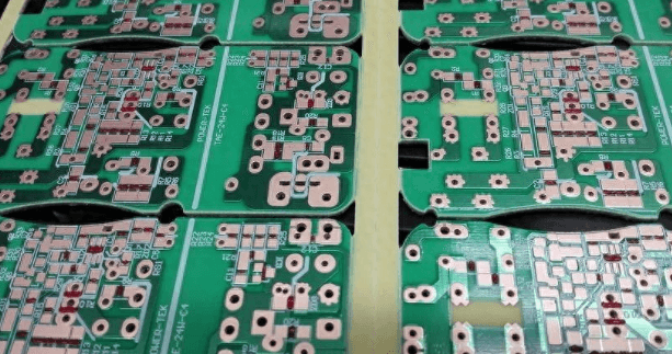
The reason why the dedicated test is dedicated is mainly because the fixture (Fixture, such as the needle plate for electrical testing of circuit boards) used is only suitable for one material number. Boards with different material numbers cannot be tested and cannot be recycled. In terms of test points, single-sided boards can be tested within 10,240 points and double-sided boards can be tested within 8,192 points. In terms of test density, due to the thickness of the probe head, it is more suitable for boards above pitch.
(2)Universal Grid Test
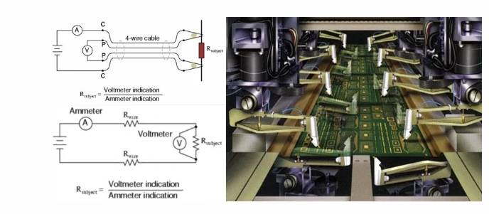
The basic principle of universal grid test is that the layout of PCB circuit is designed according to grid. Generally speaking, circuit density refers to the distance of grid, which is expressed by pitch (sometimes it can also be expressed by hole density). Universal grid test is based on this principle. According to the hole position, a G10 substrate is used as mask. Only at the hole position can the probe pass through the mask for electrical testing. Therefore, the production of fixture is simple and fast, and the probe can be reused.
Universal grid test has a large standard grid fixed needle plate with many test points. The needle plate of movable probe can be made according to different material numbers. When mass production is carried out, just replace the movable needle plate to test different material numbers. In addition, to ensure that the circuit system of the completed PCB board is unobstructed, it is necessary to use a general-purpose electrical test mother machine with high voltage (such as 250V) and multiple test points, and use a needle plate with specific contacts to perform open/short electrical tests on the board. This general-purpose test machine is called “Automatic Testing Equipment” (ATE).
The number of general-purpose test points is usually more than 10,000 points, and the test density is or is called on-grid test. If it is used for high-density boards, the spacing is too dense and it has deviated from the on-grid design, so it belongs to off-grid test, and its fixture must be specially designed. Usually, the test density of general-purpose tests can reach QFP.
(3)Flying Probe Test
The principle of flying probe test is very simple. It only requires two probes to move in x, y, and z to test the two ends of each line one by one, so there is no need to make expensive fixtures. However, since it is an endpoint test, the test speed is extremely slow, about 10~40 points/sec, so it is more suitable for samples and small-scale production. In terms of test density, flying probe testing can be applied to extremely high-density boards (), such as MCM.