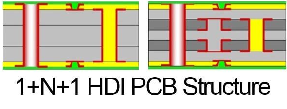
Pcb hdi 1+n+1
Advantages Of Using PCB HDI 1+N+1 In Modern Electronics
The advent of High-Density Interconnect (HDI) technology has revolutionized the field of printed circuit boards (PCBs), particularly with the introduction of the PCB HDI 1+N+1 configuration. This specific type of HDI PCB has become increasingly popular in modern electronics due to its numerous advantages, which contribute to enhanced performance, miniaturization, and reliability of electronic devices. Understanding these benefits is crucial for engineers and designers who aim to leverage cutting-edge technology in their projects.
One of the primary advantages of using PCB HDI 1+N+1 in modern electronics is the significant improvement in circuit density.
The 1+N+1 configuration refers to a structure where there is one build-up layer on each side of the core, allowing for more interconnections within a smaller area. This increased density is particularly beneficial in applications where space is at a premium, such as in smartphones, tablets, and other portable devices. By enabling more components to be placed on a single board, HDI technology facilitates the creation of compact and lightweight devices without compromising functionality.
In addition to space-saving benefits, PCB HDI 1+N+1 also enhances signal integrity.
The shorter and more direct routing paths made possible by the high-density interconnects reduce the likelihood of signal loss and electromagnetic interference (EMI). This is especially important in high-frequency applications where maintaining signal quality is critical. Consequently, devices that utilize HDI PCBs can achieve faster data transmission rates and improved overall performance, making them ideal for advanced communication systems and high-speed computing.
Moreover, the use of microvias in PCB HDI 1+N+1 designs contributes to better thermal management.
Microvias, which are smaller than traditional vias, allow for efficient heat dissipation by providing a direct path for heat to escape from the components. This is particularly advantageous in high-power applications where excessive heat can lead to component failure and reduced lifespan of the device. By effectively managing thermal loads, HDI PCBs ensure the reliability and longevity of electronic products.
Another notable advantage of PCB HDI 1+N+1 is the potential for cost savings in the long run.
Although the initial manufacturing costs of HDI PCBs may be higher compared to traditional PCBs, the benefits of reduced size, improved performance, and enhanced reliability can lead to lower overall costs. For instance, the ability to integrate more functions into a single board can reduce the need for additional components and interconnections, thereby simplifying the assembly process and reducing material costs. Additionally, the improved thermal management and signal integrity can minimize the risk of costly repairs and replacements, further contributing to cost efficiency.
Furthermore, the versatility of PCB HDI 1+N+1 makes it suitable for a wide range of applications across various industries.
From consumer electronics to automotive systems, medical devices, and aerospace technology, the advantages of HDI PCBs are being leveraged to meet the demands of increasingly complex and sophisticated electronic systems. The ability to design compact, high-performance, and reliable devices is a key factor driving the adoption of HDI technology in these sectors.
In conclusion, the advantages of using PCB HDI 1+N+1 in modern electronics are manifold, encompassing improved circuit density, enhanced signal integrity, better thermal management, potential cost savings, and versatility across various applications. As the demand for smaller, faster, and more reliable electronic devices continues to grow, the role of HDI technology in shaping the future of electronics cannot be overstated. Engineers and designers who embrace this technology will be well-positioned to create innovative solutions that meet the evolving needs of the market.
Design Considerations For PCB HDI 1+N+1 Layouts
When designing PCB HDI 1+N+1 layouts, several critical considerations must be taken into account to ensure optimal performance and reliability. High-Density Interconnect (HDI) technology, characterized by its use of microvias, blind and buried vias, and fine lines and spaces, allows for more compact and efficient circuit designs. The 1+N+1 configuration, which includes one HDI layer on each side of a core layer, presents unique challenges and opportunities that must be carefully managed.
To begin with, the selection of materials is paramount.
The dielectric materials used in HDI PCBs must possess excellent thermal and electrical properties to handle the increased density and complexity. Materials with low dielectric constants and low loss tangents are preferred to minimize signal degradation. Additionally, the coefficient of thermal expansion (CTE) should be closely matched between the dielectric and the copper to prevent delamination or cracking during thermal cycling.
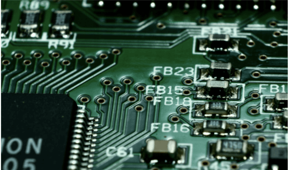
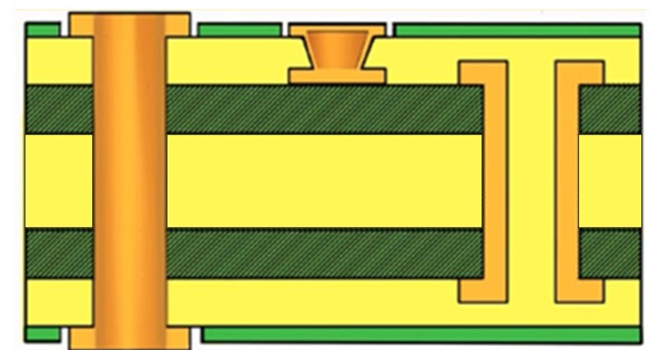
Transitioning to the aspect of via design, microvias play a crucial role in HDI PCBs.
These vias, typically laser-drilled, allow for connections between layers without consuming significant board real estate. However, their reliability is contingent upon proper design and manufacturing processes. Ensuring that microvias are properly filled and plated is essential to prevent voids and ensure robust electrical connections. Furthermore, the aspect ratio of microvias, which is the ratio of the hole depth to its diameter, should be kept within recommended limits to maintain structural integrity.
Signal integrity is another critical consideration in HDI 1+N+1 layouts.
As signal speeds increase, issues such as crosstalk, impedance mismatches, and signal attenuation become more pronounced. To mitigate these issues, careful attention must be paid to trace width, spacing, and routing. Differential pairs should be routed with consistent spacing to maintain impedance control, and ground planes should be strategically placed to provide effective return paths for high-speed signals. Additionally, the use of advanced simulation tools can help identify potential signal integrity issues early in the design process.
Thermal management is also a significant concern in HDI PCBs due to the increased component density and power consumption.
Effective heat dissipation strategies, such as the use of thermal vias, heat sinks, and thermal interface materials, are essential to prevent overheating and ensure reliable operation. Moreover, the placement of components should be optimized to facilitate natural convection and minimize thermal hotspots.
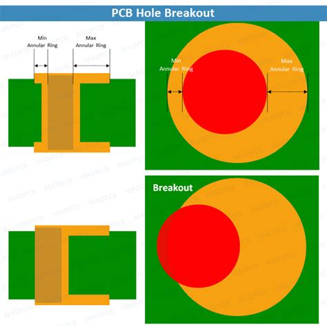
Manufacturability is another key aspect that must be considered during the design phase.
The complexity of HDI PCBs necessitates close collaboration with the PCB manufacturer to ensure that the design can be fabricated reliably and cost-effectively. Design for manufacturability (DFM) guidelines should be followed to avoid issues such as insufficient annular rings, misregistration, and insufficient solder mask clearance. Additionally, the use of automated design rule checks (DRC) can help identify potential manufacturability issues before the design is finalized.
In conclusion, designing PCB HDI 1+N+1 layouts requires a comprehensive understanding of material properties, via design, signal integrity, thermal management, and manufacturability. By carefully considering these factors and leveraging advanced design tools and collaboration with manufacturing partners, designers can create high-performance, reliable HDI PCBs that meet the demands of modern electronic applications. The intricate balance of these considerations ensures that the final product not only meets the technical specifications but also performs reliably in real-world conditions.
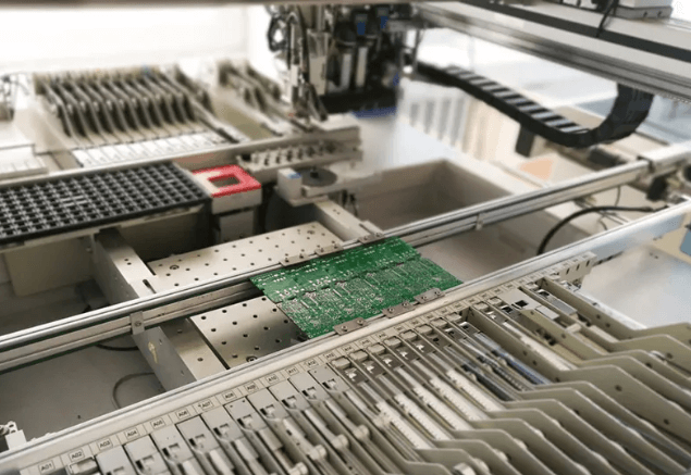
Manufacturing Challenges Of PCB HDI 1+N+1
The manufacturing of PCB HDI 1+N+1, or High-Density Interconnect printed circuit boards with a 1+N+1 structure, presents a unique set of challenges that require meticulous attention to detail and advanced technological capabilities. This specific configuration, characterized by a single layer of high-density interconnects on either side of a core layer, is increasingly favored in the electronics industry for its ability to support complex circuitry within a compact form factor. However, the intricate nature of these boards necessitates a series of precise and often demanding manufacturing processes.
One of the primary challenges in the production of PCB HDI 1+N+1 is the need for advanced materials and technologies.
The high-density interconnects require the use of fine-line circuitry and microvias, which are significantly smaller than those found in traditional PCBs. Consequently, manufacturers must employ cutting-edge laser drilling techniques to create these microvias with the necessary precision. The use of lasers, while effective, introduces its own set of complications, such as the need for stringent control over laser parameters to avoid damaging the surrounding material.
In addition to the technical demands of microvia creation, the lamination process in PCB HDI 1+N+1 manufacturing is particularly complex.
The multiple layers must be aligned with extreme accuracy to ensure the integrity of the electrical connections. Any misalignment can lead to defects that compromise the functionality of the final product. This necessitates the use of advanced alignment systems and rigorous quality control measures throughout the lamination process. Furthermore, the materials used in the lamination must be carefully selected to withstand the thermal and mechanical stresses encountered during both manufacturing and operation.
Another significant challenge is the aspect of signal integrity.
As the density of the interconnects increases, so does the potential for signal interference and loss. Manufacturers must therefore implement sophisticated design strategies to mitigate these issues. This often involves the use of advanced simulation tools to model the electrical behavior of the PCB and identify potential problem areas before physical production begins. Additionally, the choice of dielectric materials plays a crucial role in maintaining signal integrity, necessitating a careful balance between material properties and manufacturing feasibility.
Thermal management is also a critical concern in the manufacturing of PCB HDI 1+N+1.
The compact nature of these boards means that heat dissipation can become a significant issue, particularly in high-performance applications. Manufacturers must incorporate effective thermal management solutions, such as thermal vias and heat sinks, into the design. This requires a thorough understanding of thermal dynamics and the ability to integrate these solutions without compromising the board’s structural integrity or electrical performance.
Moreover, the inspection and testing of PCB HDI 1+N+1 boards are more challenging compared to traditional PCBs.
The high density and complexity of the interconnects make it difficult to detect defects using conventional inspection methods. Advanced techniques such as automated optical inspection (AOI) and X-ray inspection are often required to ensure the quality and reliability of the final product. These methods, while effective, add to the overall cost and time required for manufacturing.
In conclusion, the manufacturing of PCB HDI 1+N+1 involves a series of intricate and demanding processes that require advanced materials, technologies, and design strategies.
From the creation of microvias to the management of signal integrity and thermal dynamics, each step presents its own set of challenges that must be meticulously addressed to produce a high-quality, reliable product. As the demand for compact and high-performance electronic devices continues to grow, the ability to overcome these manufacturing challenges will be crucial for the continued advancement of PCB technology.
Applications Of PCB HDI 1+N+1 In Consumer Electronics
The advent of High-Density Interconnect (HDI) technology has revolutionized the landscape of printed circuit boards (PCBs), particularly in the realm of consumer electronics. Among the various configurations of HDI PCBs, the 1+N+1 structure stands out due to its unique design and versatile applications. This configuration, characterized by a single layer of microvias on both the top and bottom layers of the PCB, sandwiching multiple layers of buried vias, offers a compelling combination of performance, reliability, and compactness. Consequently, it has found widespread use in a variety of consumer electronic devices.
One of the primary applications of PCB HDI 1+N+1 is in smartphones.
The demand for slimmer, more powerful, and feature-rich smartphones has driven manufacturers to adopt advanced PCB technologies. The 1+N+1 configuration allows for a higher density of interconnections, enabling more components to be packed into a smaller area. This not only reduces the overall size of the device but also enhances its performance by shortening the signal paths, thereby reducing latency and power consumption. Furthermore, the improved thermal management capabilities of HDI PCBs ensure that smartphones can operate efficiently even under heavy usage.
In addition to smartphones, wearable technology has also benefited significantly from the adoption of PCB HDI 1+N+1.
Devices such as smartwatches and fitness trackers require compact and lightweight components without compromising on functionality. The high-density interconnects provided by the 1+N+1 structure facilitate the integration of various sensors, processors, and communication modules within a limited space. This enables wearables to offer a wide range of features, from health monitoring to GPS tracking, while maintaining a sleek and ergonomic design.
Moreover, the application of PCB HDI 1+N+1 extends to the realm of tablets and laptops.
As these devices continue to evolve, there is a growing emphasis on enhancing their processing power and battery life while minimizing their form factor. The 1+N+1 configuration supports the integration of advanced processors, memory modules, and other critical components in a compact layout. This not only improves the overall performance of tablets and laptops but also contributes to their portability and user convenience. Additionally, the robust construction of HDI PCBs ensures durability and reliability, which are essential for devices that are frequently used and transported.
Another notable application of PCB HDI 1+N+1 is in the field of gaming consoles.
Modern gaming consoles demand high-speed data processing and efficient power management to deliver an immersive gaming experience. The 1+N+1 structure, with its high interconnect density and superior electrical performance, is well-suited to meet these requirements. It allows for the integration of powerful graphics processors, memory units, and other critical components, ensuring smooth and responsive gameplay. Furthermore, the enhanced thermal management capabilities of HDI PCBs help in maintaining optimal operating temperatures, thereby preventing overheating and ensuring the longevity of the gaming console.
In conclusion, the PCB HDI 1+N+1 configuration has become an integral component in the design and development of various consumer electronic devices. Its ability to support high-density interconnections, coupled with its compact and robust design, makes it an ideal choice for applications ranging from smartphones and wearables to tablets, laptops, and gaming consoles. As consumer electronics continue to advance, the role of HDI PCBs, particularly the 1+N+1 structure, will undoubtedly become even more critical in meeting the ever-evolving demands for performance, reliability, and miniaturization.