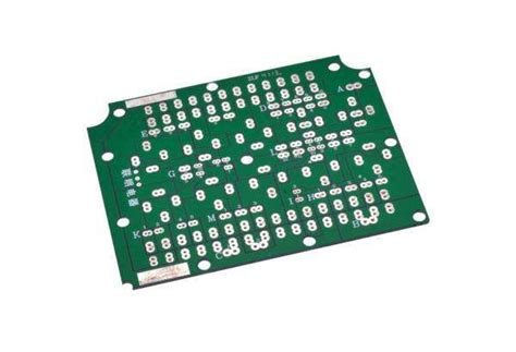
Pcb heat sink pad
Advantages Of Using Heavy Copper In PCB Design
Heavy copper in printed circuit board (PCB) design offers a multitude of advantages that significantly enhance the performance, reliability, and durability of electronic devices. As the demand for more robust and efficient electronic components continues to grow, the utilization of heavy copper in PCBs has become increasingly prevalent. This article delves into the various benefits associated with incorporating heavy copper into PCB design, providing a comprehensive understanding of its impact on modern electronics.
One of the primary advantages of using heavy copper in PCB design is its ability to handle higher current loads.
Traditional PCBs, which typically use thin copper layers, are often limited in their current-carrying capacity. In contrast, heavy copper PCBs, with copper thicknesses ranging from 3 oz/ft² to over 10 oz/ft², can manage significantly higher currents without the risk of overheating or failure. This capability is particularly crucial in applications such as power supplies, automotive electronics, and industrial machinery, where high current loads are commonplace.
Moreover, heavy copper PCBs exhibit superior thermal management properties.
The increased copper thickness allows for more efficient heat dissipation, which is essential in preventing thermal buildup that can damage components and reduce the overall lifespan of the device. By effectively managing heat, heavy copper PCBs contribute to the stability and reliability of electronic systems, ensuring consistent performance even under demanding conditions. This thermal advantage is especially beneficial in high-power applications, such as electric vehicles and renewable energy systems, where efficient heat management is critical.
In addition to handling higher currents and improving thermal management, heavy copper PCBs also offer enhanced mechanical strength.
The thicker copper layers provide greater structural integrity, making the PCB more resistant to mechanical stresses such as bending, vibration, and thermal cycling. This increased durability is vital in environments where electronic devices are subjected to harsh conditions, such as aerospace, military, and industrial applications. By withstanding these stresses, heavy copper PCBs help to minimize the risk of failure and extend the operational life of the device.
Furthermore, the use of heavy copper in PCB design allows for more complex and compact circuit layouts.
The ability to carry higher currents through thicker copper traces means that designers can reduce the number of layers required in a PCB, leading to more compact and efficient designs. This reduction in layer count not only simplifies the manufacturing process but also lowers production costs. Additionally, the increased current-carrying capacity enables the integration of more components on a single board, further enhancing the functionality and performance of the device.
Another notable advantage of heavy copper PCBs is their improved reliability in high-frequency applications.
The thicker copper layers reduce the impedance of the traces, which is crucial for maintaining signal integrity in high-frequency circuits. This reduction in impedance helps to minimize signal loss and electromagnetic interference (EMI), ensuring that the device operates efficiently and accurately. High-frequency applications, such as telecommunications and advanced computing systems, greatly benefit from the enhanced performance provided by heavy copper PCBs.
In conclusion, the incorporation of heavy copper in PCB design offers a range of significant advantages that contribute to the overall performance, reliability, and durability of electronic devices. By enabling higher current-carrying capacity, superior thermal management, enhanced mechanical strength, more complex circuit layouts, and improved reliability in high-frequency applications, heavy copper PCBs have become an indispensable component in the advancement of modern electronics. As technology continues to evolve, the demand for heavy copper PCBs is expected to grow, further solidifying their importance in the development of cutting-edge electronic systems.
Manufacturing Techniques For Heavy Copper PCBs
Manufacturing techniques for heavy copper PCBs have evolved significantly over the years, driven by the increasing demand for high-performance electronic devices capable of handling substantial electrical currents. Heavy copper PCBs, characterized by copper thicknesses exceeding 3 ounces per square foot, are essential in applications requiring enhanced thermal management and mechanical strength. The manufacturing process for these robust circuit boards involves several critical steps, each contributing to the overall reliability and functionality of the final product.
To begin with, the selection of appropriate base materials is crucial.
Heavy copper PCBs typically utilize high-temperature laminates, such as FR-4 or polyimide, which can withstand the elevated thermal stresses associated with thick copper layers. These materials provide a stable foundation, ensuring that the PCB maintains its structural integrity throughout the manufacturing process and during operation. Once the base material is chosen, the next step involves the application of the copper layers.
Electroplating is a common technique used to achieve the desired copper thickness.
This process involves immersing the PCB in an electrolytic solution and applying an electric current, which causes copper ions to deposit onto the board’s surface. By carefully controlling the current density and plating time, manufacturers can achieve uniform copper layers with the required thickness. However, electroplating alone may not be sufficient for extremely thick copper layers, necessitating the use of additional techniques.
Lamination is another critical step in the manufacturing process.
In this stage, multiple layers of copper and dielectric materials are bonded together under high pressure and temperature. This process not only increases the overall copper thickness but also enhances the mechanical strength and thermal conductivity of the PCB. The lamination process must be meticulously controlled to prevent defects such as delamination or voids, which could compromise the board’s performance.
Following lamination, the PCB undergoes a series of etching processes to define the circuit patterns.
Traditional etching techniques, such as chemical etching, may not be suitable for heavy copper PCBs due to the increased copper thickness. Instead, manufacturers often employ advanced etching methods, such as plasma etching or laser ablation, which offer greater precision and control. These techniques allow for the creation of intricate circuit patterns while minimizing the risk of over-etching or under-etching.
Once the circuit patterns are defined, the PCB is subjected to a series of finishing processes to enhance its durability and performance.
Surface finishes, such as hot air solder leveling (HASL) or electroless nickel immersion gold (ENIG), are applied to protect the copper traces from oxidation and improve solderability. Additionally, solder masks and silkscreens are added to provide insulation and labeling, respectively.
Quality control is an integral part of the manufacturing process for heavy copper PCBs.
Rigorous testing, including electrical testing, thermal cycling, and mechanical stress testing, is conducted to ensure that the PCB meets the required specifications and can withstand the demanding conditions of its intended application. Any defects or inconsistencies identified during testing are addressed promptly to maintain the highest standards of quality and reliability.
In conclusion, the manufacturing techniques for heavy copper PCBs involve a series of meticulously controlled processes, from material selection and electroplating to lamination, etching, and finishing. Each step plays a vital role in ensuring the final product’s performance, durability, and reliability. As technology continues to advance, the demand for heavy copper PCBs is expected to grow, driving further innovations in manufacturing techniques to meet the evolving needs of high-performance electronic devices.
Applications Of Heavy Copper PCBs In High-Power Devices
Heavy copper PCBs, characterized by their thick copper layers, are increasingly becoming indispensable in the realm of high-power devices. These specialized printed circuit boards are designed to handle higher currents and dissipate heat more efficiently than standard PCBs, making them ideal for applications that demand robust performance and reliability. The utilization of heavy copper PCBs in high-power devices is driven by their unique ability to manage thermal and electrical loads, which is critical in various industrial and technological sectors.
One of the primary applications of heavy copper PCBs is in power supply systems.
These systems require components that can handle substantial electrical currents without overheating or failing. Heavy copper PCBs are well-suited for this purpose due to their enhanced thermal management capabilities. The thick copper layers facilitate efficient heat dissipation, thereby preventing the components from reaching critical temperatures. This ensures the longevity and reliability of power supply systems, which are essential for the uninterrupted operation of various electronic devices and machinery.
In addition to power supply systems, heavy copper PCBs are extensively used in automotive electronics.
Modern vehicles are equipped with numerous electronic systems that control everything from engine performance to safety features. These systems often operate under high current loads and generate significant amounts of heat. Heavy copper PCBs provide the necessary durability and thermal management to ensure these systems function optimally. For instance, electric vehicles (EVs) rely heavily on heavy copper PCBs for their battery management systems, inverters, and charging stations. The ability of these PCBs to handle high currents and dissipate heat effectively is crucial for the performance and safety of EVs.
Another significant application of heavy copper PCBs is in industrial control systems.
These systems are used to monitor and control industrial processes, often in harsh environments where reliability is paramount. Heavy copper PCBs are capable of withstanding high temperatures and mechanical stresses, making them ideal for use in industrial control systems. They ensure that the electronic components can handle the demanding conditions without compromising performance. This is particularly important in industries such as manufacturing, where any failure in the control systems can lead to costly downtime and production losses.
Furthermore, heavy copper PCBs are also employed in renewable energy systems, such as solar power and wind power installations.
These systems require efficient power conversion and distribution to maximize energy output. Heavy copper PCBs are used in the inverters and converters that transform the generated energy into usable electrical power. Their ability to handle high currents and dissipate heat efficiently ensures that these renewable energy systems operate at peak efficiency, contributing to the overall sustainability and reliability of the energy supply.
In the realm of telecommunications, heavy copper PCBs play a crucial role in the infrastructure that supports high-speed data transmission.
The increasing demand for faster and more reliable communication networks necessitates the use of components that can handle high power loads and maintain signal integrity. Heavy copper PCBs provide the necessary performance characteristics to meet these demands, ensuring that telecommunications equipment operates efficiently and reliably.
In conclusion, the applications of heavy copper PCBs in high-power devices are vast and varied. Their ability to manage high currents and dissipate heat effectively makes them indispensable in power supply systems, automotive electronics, industrial control systems, renewable energy installations, and telecommunications infrastructure. As technology continues to advance and the demand for high-power devices grows, the importance of heavy copper PCBs in ensuring the reliability and performance of these devices cannot be overstated.
Thermal Management Solutions With Heavy Copper PCBs
In the realm of modern electronics, thermal management has emerged as a critical concern, particularly as devices become more powerful and compact. One innovative solution that has gained traction is the use of heavy copper printed circuit boards (PCBs). These specialized PCBs are designed to handle higher current loads and dissipate heat more effectively than their standard counterparts, making them indispensable in applications where thermal management is paramount.
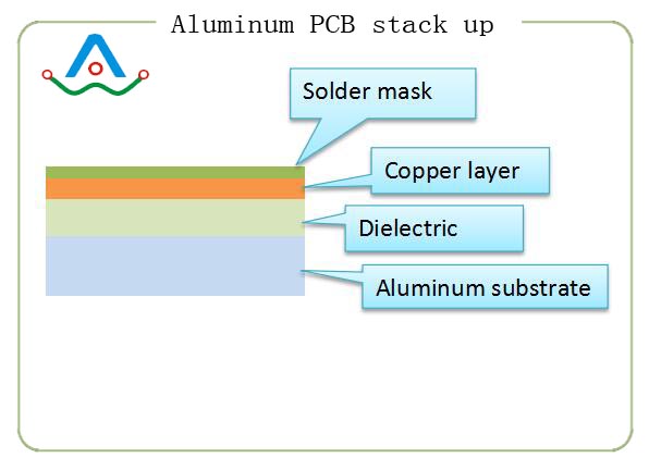
Heavy copper PCBs are characterized by their thicker copper layers, which typically range from 105 to 400 micrometers, compared to the 18 to 70 micrometers found in standard PCBs. This increased copper thickness allows for enhanced current-carrying capacity and improved heat dissipation. Consequently, these PCBs are particularly well-suited for high-power applications such as power supplies, automotive electronics, and industrial control systems.
One of the primary advantages of heavy copper PCBs is their ability to manage thermal loads efficiently.
As electronic components generate heat during operation, it is crucial to dissipate this heat to prevent overheating and ensure reliable performance. Heavy copper PCBs excel in this regard due to their superior thermal conductivity. The thicker copper layers facilitate the rapid transfer of heat away from critical components, thereby reducing the risk of thermal damage and extending the lifespan of the device.
Moreover, heavy copper PCBs offer enhanced mechanical strength, which is particularly beneficial in harsh environments.
The robust construction of these PCBs makes them more resistant to thermal cycling and mechanical stress, ensuring long-term reliability even under demanding conditions. This durability is especially important in applications such as aerospace and military electronics, where failure is not an option.
In addition to their thermal and mechanical advantages, heavy copper PCBs also provide design flexibility.
Engineers can incorporate complex and dense circuitry without compromising performance, thanks to the increased current-carrying capacity of the thicker copper layers. This flexibility allows for the development of more compact and efficient devices, which is a significant advantage in the ever-evolving landscape of electronic design.
Furthermore, the use of heavy copper PCBs can lead to cost savings in the long run.
While the initial manufacturing cost may be higher compared to standard PCBs, the improved thermal management and reliability can reduce the need for additional cooling solutions and maintenance. This reduction in ancillary components and maintenance efforts translates to lower overall costs and increased efficiency.
It is also worth noting that advancements in manufacturing techniques have made heavy copper PCBs more accessible.
Innovations such as electroplating and etching processes have streamlined production, enabling the creation of intricate designs with high precision. These advancements have not only improved the quality of heavy copper PCBs but have also made them more cost-effective, further driving their adoption in various industries.
In conclusion, heavy copper PCBs represent a significant advancement in thermal management solutions for modern electronics. Their superior thermal conductivity, mechanical strength, and design flexibility make them an ideal choice for high-power applications. As technology continues to evolve, the demand for efficient and reliable thermal management solutions will only increase, solidifying the role of heavy copper PCBs in the future of electronic design