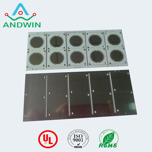
Pcb heavy copper
Advantages Of Using Pcb heavy copper Design
Heavy copper in printed circuit board (PCB) design offers a multitude of advantages that significantly enhance the performance, reliability, and durability of electronic devices.
One of the primary benefits of using heavy copper in PCB design is its ability to handle higher current loads.
Traditional PCBs, which typically use copper traces with a thickness of 1 oz/ft², may struggle to manage high current applications. In contrast, heavy copper PCBs, with copper thicknesses ranging from 3 oz/ft² to 20 oz/ft² or more, can efficiently conduct higher currents without overheating or suffering from excessive voltage drops. This capability is particularly crucial in power electronics, automotive, and industrial applications where robust current handling is essential.
Moreover, heavy copper PCBs exhibit superior thermal management properties.
The increased copper thickness allows for better heat dissipation, which is vital in preventing thermal buildup that can damage components and reduce the overall lifespan of the device. Effective thermal management ensures that the PCB operates within safe temperature ranges, thereby enhancing the reliability and performance of the electronic system. This is especially important in high-power applications where heat generation is a significant concern.
In addition to improved current handling and thermal management, heavy copper PCBs offer enhanced mechanical strength.
The thicker copper layers provide greater structural integrity, making the PCB more resistant to mechanical stresses such as bending, vibration, and thermal cycling. This increased durability is beneficial in harsh environments where electronic devices are subjected to rigorous conditions. For instance, in automotive and aerospace applications, where reliability and longevity are paramount, heavy copper PCBs can withstand the demanding operational environments better than their standard counterparts.
Furthermore, the use of heavy copper in PCB design allows for more complex and compact circuit layouts.
Designers can incorporate finer traces and spaces, enabling the creation of intricate circuits that would be challenging to achieve with standard copper thicknesses. This capability is advantageous in modern electronic devices that require high-density interconnections and miniaturization. By utilizing heavy copper, designers can optimize the PCB layout to achieve better performance and functionality without compromising on space or reliability.
Another significant advantage of heavy copper PCBs is their ability to support advanced thermal vias and heat sinks.
These features are essential for managing heat in high-power applications. Thermal vias, which are vertical interconnections filled with copper, facilitate efficient heat transfer from the surface of the PCB to the inner layers or to an external heat sink. This efficient heat dissipation mechanism helps maintain optimal operating temperatures, thereby preventing thermal damage and ensuring the longevity of the electronic components.
Additionally, heavy copper PCBs are highly customizable, allowing designers to tailor the PCB to meet specific application requirements.
The flexibility in design and manufacturing processes enables the creation of PCBs with varying copper thicknesses, layer counts, and configurations. This customization ensures that the PCB can meet the unique demands of different applications, providing a tailored solution that maximizes performance and reliability.
In conclusion, the advantages of using heavy copper in PCB design are manifold, encompassing improved current handling, superior thermal management, enhanced mechanical strength, and the ability to support complex circuit layouts. These benefits make heavy copper PCBs an ideal choice for high-power, high-reliability applications across various industries. By leveraging the unique properties of heavy copper, designers can create robust, efficient, and durable electronic systems that meet the stringent demands of modern technology.
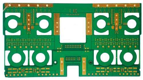
Manufacturing Techniques For Heavy Copper PCBs
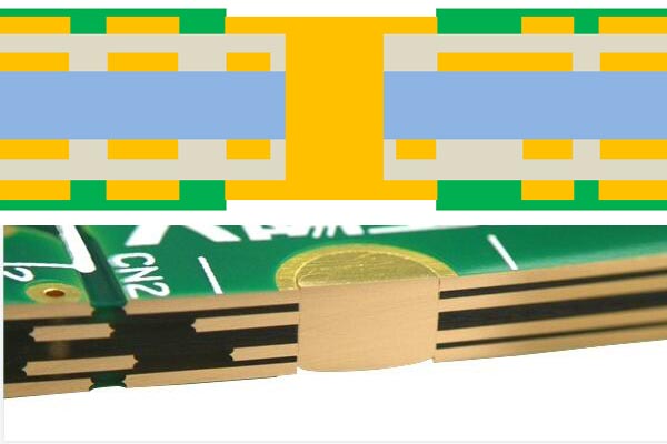
Heavy copper PCBs, characterized by their thick copper layers, are essential in applications requiring high current carrying capacity and enhanced thermal management. The manufacturing techniques for these robust circuit boards are more complex than those for standard PCBs, necessitating specialized processes to ensure reliability and performance. Understanding these techniques is crucial for engineers and manufacturers aiming to leverage the benefits of heavy copper PCBs in demanding environments.
The initial step in manufacturing heavy copper PCBs involves selecting the appropriate base material.
Typically, FR4, a glass-reinforced epoxy laminate, is used due to its excellent mechanical and electrical properties. However, for heavy copper applications, the base material must be able to withstand the additional thermal and mechanical stresses imposed by the thick copper layers. Once the base material is chosen, the next phase is the application of the copper layers.
In standard PCB manufacturing, copper layers are typically applied using a process called electroless copper deposition, followed by electroplating.
However, for heavy copper PCBs, the copper layers are significantly thicker, often exceeding 3 ounces per square foot. This necessitates a more robust electroplating process, where multiple layers of copper are deposited to achieve the desired thickness. The electroplating process must be carefully controlled to ensure uniform thickness and to prevent issues such as voids or uneven deposition, which can compromise the board’s performance.
Following the electroplating process, the next critical step is the etching of the copper layers to create the desired circuit patterns.
In heavy copper PCB manufacturing, the etching process must be meticulously managed to handle the thicker copper layers. Traditional etching solutions may not be sufficient, requiring the use of more aggressive etching chemicals or extended etching times. Additionally, the etching process must ensure that the edges of the copper traces are smooth and free of burrs, which can cause electrical shorts or other issues.
Once the etching is complete, the next phase involves the application of solder mask and silkscreen.
The solder mask, a protective layer applied over the copper traces, must be able to adhere well to the thicker copper layers and provide adequate protection against oxidation and environmental factors. The silkscreen, used for labeling and identifying components on the PCB, must also be applied with precision to ensure readability and accuracy.
Another critical aspect of heavy copper PCB manufacturing is the drilling and plating of vias, which are the holes that connect different layers of the PCB.
In heavy copper PCBs, the vias must be able to handle higher currents and thermal loads, necessitating the use of specialized drilling techniques and plating processes. The vias are typically filled with conductive materials, such as copper or silver, to enhance their current-carrying capacity and thermal conductivity.
Finally, the completed heavy copper PCB undergoes rigorous testing and inspection to ensure it meets the required specifications and performance standards. This includes electrical testing to verify the integrity of the circuits, as well as thermal and mechanical testing to ensure the board can withstand the operating conditions it will be subjected to.
In conclusion, the manufacturing techniques for heavy copper PCBs are complex and require careful attention to detail at every stage of the process. From selecting the appropriate base material to applying and etching the thick copper layers, each step must be meticulously managed to ensure the final product meets the demanding requirements of high-current and high-thermal applications. By understanding and implementing these techniques, manufacturers can produce reliable and high-performance heavy copper PCBs that are essential for a wide range of industrial and commercial applications.
Applications Of Heavy Copper PCBs In High-Power Electronics
Heavy copper PCBs, characterized by their thick copper layers, are increasingly becoming indispensable in the realm of high-power electronics. These specialized printed circuit boards (PCBs) are designed to handle higher currents and dissipate heat more effectively than standard PCBs, making them ideal for a variety of demanding applications. As the demand for more robust and reliable electronic devices continues to grow, the applications of heavy copper PCBs are expanding across multiple industries.
One of the primary applications of heavy copper PCBs is in power supply systems.
These systems require components that can manage high current loads without overheating or failing. Heavy copper PCBs are well-suited for this purpose due to their enhanced thermal management capabilities. The thick copper layers allow for efficient heat dissipation, ensuring that the components remain within safe operating temperatures. This is particularly crucial in uninterruptible power supplies (UPS) and power distribution units (PDUs), where reliability and performance are paramount.
In addition to power supply systems, heavy copper PCBs are also extensively used in the automotive industry.
Modern vehicles are equipped with a multitude of electronic systems, ranging from engine control units (ECUs) to advanced driver-assistance systems (ADAS). These systems often operate under high current conditions and require robust PCBs to ensure their reliability and longevity. Heavy copper PCBs provide the necessary durability and thermal management, making them an ideal choice for automotive applications. Furthermore, the ability to handle high currents makes these PCBs suitable for electric vehicles (EVs), where efficient power management is critical.
Another significant application of heavy copper PCBs is in industrial control systems.
These systems often operate in harsh environments and are subject to high levels of electrical and thermal stress. Heavy copper PCBs can withstand these conditions, providing reliable performance and reducing the risk of system failures. They are commonly used in motor controllers, industrial power converters, and other high-power industrial equipment. The robustness of heavy copper PCBs ensures that these systems can operate efficiently and safely, even under extreme conditions.
Moreover, heavy copper PCBs are also finding applications in renewable energy systems.
Solar power inverters and wind turbine controllers are examples of systems that require efficient power management and high reliability. Heavy copper PCBs can handle the high currents generated by these renewable energy sources, ensuring efficient energy conversion and distribution. The enhanced thermal management capabilities of these PCBs also help in maintaining the performance and longevity of the renewable energy systems.
In the realm of telecommunications, heavy copper PCBs are used in high-power amplifiers and base stations.
These components require efficient heat dissipation to maintain signal integrity and prevent overheating. Heavy copper PCBs provide the necessary thermal management, ensuring reliable performance and reducing the risk of signal degradation. This is particularly important in the era of 5G technology, where high-power components are essential for maintaining fast and reliable communication networks.
In conclusion, the applications of heavy copper PCBs in high-power electronics are vast and varied. From power supply systems and automotive electronics to industrial control systems and renewable energy, these robust PCBs play a crucial role in ensuring the reliability and efficiency of high-power electronic devices. As technology continues to advance, the demand for heavy copper PCBs is expected to grow, further solidifying their importance in the field of high-power electronics.

Cost Considerations And Benefits Of Heavy Copper PCBs
When evaluating the cost considerations and benefits of heavy copper PCBs, it is essential to understand the unique attributes that distinguish them from standard PCBs. Heavy copper PCBs, characterized by their thicker copper layers, typically ranging from 3 oz/ft² to 20 oz/ft², offer enhanced performance in high-current applications and harsh environments. However, these advantages come with specific cost implications that must be carefully weighed against the benefits.
One of the primary cost considerations associated with heavy copper PCBs is the increased material expense.
The thicker copper layers require more raw copper, which directly impacts the overall cost of the PCB. Additionally, the manufacturing process for heavy copper PCBs is more complex and time-consuming compared to standard PCBs. Specialized equipment and techniques, such as high-temperature lamination and advanced etching processes, are necessary to handle the thicker copper layers. These additional steps contribute to higher production costs, which can be a significant factor for companies operating within tight budget constraints.
Despite the higher initial costs, the benefits of heavy copper PCBs often justify the investment, particularly in applications where reliability and performance are paramount.
One of the most notable advantages is their ability to handle higher current loads without experiencing excessive heat buildup. This capability is crucial in power electronics, automotive, and industrial applications, where efficient heat dissipation and robust performance are essential. The enhanced thermal management provided by heavy copper PCBs can lead to longer component lifespans and reduced risk of failure, ultimately resulting in lower maintenance and replacement costs over time.
Moreover, heavy copper PCBs offer superior mechanical strength and durability, making them well-suited for use in harsh environments.
The thicker copper layers provide increased resistance to thermal cycling, mechanical stress, and chemical exposure, which are common challenges in industrial and military applications. This enhanced durability translates to improved reliability and longevity of the electronic devices, further offsetting the initial cost premium associated with heavy copper PCBs.
Another significant benefit of heavy copper PCBs is their ability to support more complex and compact designs.
The increased current-carrying capacity allows for the integration of multiple power and ground planes within a single PCB, reducing the need for additional layers and simplifying the overall design. This capability can lead to more efficient use of space and potentially lower assembly costs, as fewer components and interconnections are required. Additionally, the improved thermal performance can enable higher power densities, allowing for more compact and efficient electronic devices.
In conclusion, while the cost considerations of heavy copper PCBs are undeniably higher due to increased material expenses and more complex manufacturing processes, the benefits they offer in terms of performance, reliability, and design flexibility often outweigh these initial costs. For applications that demand high current handling, superior thermal management, and robust durability, heavy copper PCBs present a compelling solution that can lead to long-term cost savings and enhanced device performance. Therefore, it is crucial for companies to carefully assess their specific requirements and weigh the potential benefits against the associated costs when considering the adoption of heavy copper PCBs in their electronic designs.