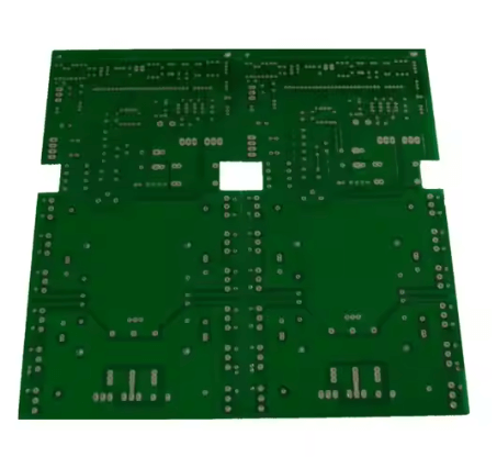
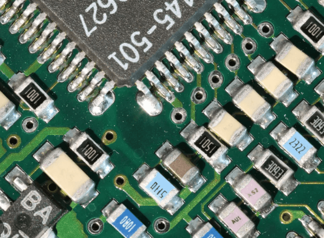
Pcb heavy copper electronic
Advantages Of Using Heavy Copper In PCB Design
The utilization of heavy copper in printed circuit board (PCB) design has garnered significant attention in recent years, primarily due to its numerous advantages that enhance the performance and reliability of electronic devices. Heavy copper PCBs, characterized by copper thicknesses exceeding 3 ounces per square foot, offer a range of benefits that make them indispensable in various high-power and high-reliability applications. As we delve into the advantages of using heavy copper in PCB design, it becomes evident that these benefits are multifaceted, impacting both the electrical and mechanical aspects of the circuit boards.
One of the foremost advantages of heavy copper PCBs is their ability to handle higher current loads.
Traditional PCBs with standard copper thicknesses often struggle to manage high current levels, leading to overheating and potential failure. In contrast, heavy copper PCBs can efficiently conduct higher currents without significant temperature rise, thereby ensuring the stability and longevity of the electronic components. This capability is particularly crucial in power electronics, automotive, and industrial applications where high current handling is a fundamental requirement.
Moreover, heavy copper PCBs exhibit superior thermal management properties.
The increased copper thickness facilitates better heat dissipation, which is essential for maintaining optimal operating temperatures of electronic devices. Effective thermal management not only enhances the performance of the components but also extends their lifespan by preventing thermal stress and degradation. Consequently, heavy copper PCBs are highly sought after in applications that demand robust thermal performance, such as power supplies, motor controllers, and LED lighting systems.
In addition to electrical and thermal advantages, heavy copper PCBs also offer enhanced mechanical strength.
The thicker copper layers provide greater structural integrity, making the PCBs more resistant to mechanical stresses and environmental factors. This increased durability is particularly beneficial in harsh operating conditions, such as those encountered in aerospace, military, and industrial environments. The ability to withstand mechanical shocks, vibrations, and extreme temperatures ensures that heavy copper PCBs maintain their functionality and reliability over extended periods.
Furthermore, the use of heavy copper in PCB design allows for more flexible and innovative circuit layouts.
Designers can incorporate complex and dense circuitry without compromising on performance or reliability. The thicker copper layers enable the creation of intricate power distribution networks and the integration of multiple functions on a single board. This design flexibility is instrumental in developing compact and efficient electronic devices that meet the ever-evolving demands of modern technology.
Another noteworthy advantage of heavy copper PCBs is their potential for cost savings in the long run.
Although the initial manufacturing cost of heavy copper PCBs may be higher compared to standard PCBs, their enhanced performance and durability can lead to significant cost reductions over the product’s lifecycle. The reduced need for additional cooling solutions, lower maintenance requirements, and extended operational life contribute to overall cost efficiency, making heavy copper PCBs a prudent investment for high-reliability applications.
In conclusion, the advantages of using heavy copper in PCB design are manifold, encompassing improved current handling, superior thermal management, enhanced mechanical strength, design flexibility, and long-term cost savings. These benefits collectively underscore the importance of heavy copper PCBs in advancing the capabilities and reliability of electronic devices across various industries. As technology continues to evolve, the role of heavy copper in PCB design is poised to become even more critical, driving innovation and excellence in electronic engineering.
Manufacturing Techniques For Heavy Copper PCBs
Manufacturing heavy copper PCBs involves a series of specialized techniques that distinguish it from the production of standard PCBs. Heavy copper PCBs, characterized by their thicker copper layers, are designed to handle higher currents and provide enhanced thermal management, making them ideal for applications in power electronics, automotive, and industrial control systems. The manufacturing process begins with the selection of appropriate base materials, typically high-temperature laminates that can withstand the increased thermal and mechanical stresses associated with heavy copper layers.
One of the initial steps in the manufacturing process is the preparation of the copper-clad laminate.
This involves cleaning and roughening the surface to ensure proper adhesion of the subsequent layers. The copper foil used in heavy copper PCBs is significantly thicker, often ranging from 3 oz/ft² to 20 oz/ft² or more, compared to the standard 1 oz/ft² used in conventional PCBs. This increased thickness necessitates the use of specialized etching techniques to accurately define the circuit patterns.
Etching heavy copper layers requires a more robust approach than standard PCBs.
Traditional etching methods may not be sufficient to remove the excess copper without causing undercutting or other defects. Therefore, manufacturers often employ a combination of chemical and mechanical etching processes. Chemical etching involves the use of strong acids or alkaline solutions to dissolve the unwanted copper, while mechanical etching may include techniques such as milling or laser ablation to achieve precise patterning.
Following the etching process, the next critical step is the application of additional copper layers through electroplating.
Electroplating involves immersing the etched PCB in an electrolytic bath and applying an electric current to deposit copper onto the exposed areas. This step is crucial for building up the copper thickness to the desired level, especially in areas such as vias and pads that require enhanced conductivity and mechanical strength. The electroplating process must be carefully controlled to ensure uniform deposition and avoid issues such as voids or uneven thickness.
Once the desired copper thickness is achieved, the PCB undergoes a series of finishing processes to enhance its durability and performance.
These processes may include the application of solder masks, which protect the copper traces from oxidation and provide insulation between conductive elements. Additionally, surface finishes such as HASL (Hot Air Solder Leveling), ENIG (Electroless Nickel Immersion Gold), or OSP (Organic Solderability Preservatives) are applied to improve solderability and protect the copper from environmental factors.
Quality control is an integral part of the manufacturing process for heavy copper PCBs.
Rigorous testing and inspection procedures are implemented to ensure that the PCBs meet the required specifications and performance standards. This may include electrical testing to verify continuity and isolation, as well as thermal cycling tests to assess the PCB’s ability to withstand temperature variations. Advanced inspection techniques such as X-ray imaging and automated optical inspection (AOI) are also employed to detect any defects or inconsistencies.
In conclusion, the manufacturing of heavy copper PCBs involves a series of specialized techniques that address the unique challenges posed by thicker copper layers. From the selection of high-temperature laminates to the precise etching and electroplating processes, each step is meticulously controlled to ensure the production of high-quality, reliable PCBs capable of handling demanding applications. The integration of advanced finishing and quality control measures further enhances the performance and longevity of these critical components in various high-power and high-reliability electronic systems.
Applications Of Heavy Copper PCBs In High-Power Electronics
Heavy copper PCBs, characterized by their thick copper layers, are increasingly becoming indispensable in the realm of high-power electronics. These specialized printed circuit boards are designed to handle higher currents and dissipate heat more efficiently than standard PCBs, making them ideal for a variety of demanding applications. The unique properties of heavy copper PCBs enable them to perform reliably in environments where conventional PCBs would fail, thus ensuring the longevity and efficiency of high-power electronic devices.
One of the primary applications of heavy copper PCBs is in power supplies.
Power supply units, especially those used in industrial settings, require robust and reliable components to manage high currents and voltages. Heavy copper PCBs are capable of withstanding these extreme conditions due to their enhanced thermal management and current-carrying capacity. This makes them an excellent choice for power conversion systems, uninterruptible power supplies (UPS), and other high-power applications where efficiency and reliability are paramount.
In addition to power supplies, heavy copper PCBs are also extensively used in automotive electronics.
Modern vehicles are equipped with a multitude of electronic systems that control everything from engine performance to safety features. These systems often operate under high current loads and generate significant amounts of heat. Heavy copper PCBs can effectively manage these thermal and electrical demands, ensuring that automotive electronic systems function optimally. This is particularly important in electric and hybrid vehicles, where efficient power management is crucial for performance and battery life.
Another significant application of heavy copper PCBs is in renewable energy systems.
Solar power inverters and wind turbine controllers are examples of renewable energy technologies that benefit from the use of heavy copper PCBs. These systems require efficient power conversion and distribution to maximize energy output and minimize losses. The superior thermal and electrical properties of heavy copper PCBs make them well-suited for these applications, contributing to the overall efficiency and reliability of renewable energy systems.
Furthermore, heavy copper PCBs are also utilized in the aerospace and defense industries.
Electronic systems used in these sectors must endure harsh environmental conditions, including extreme temperatures, vibrations, and mechanical stresses. Heavy copper PCBs provide the necessary durability and reliability to withstand these challenges. They are used in a variety of applications, including radar systems, communication equipment, and avionics, where failure is not an option.
Moreover, heavy copper PCBs find applications in industrial machinery and equipment.
High-power motor drives, welding equipment, and industrial automation systems often require PCBs that can handle high currents and dissipate heat effectively. Heavy copper PCBs meet these requirements, ensuring that industrial equipment operates efficiently and reliably. This is particularly important in manufacturing environments where downtime can result in significant financial losses.
In conclusion, the applications of heavy copper PCBs in high-power electronics are vast and varied. Their ability to handle high currents, manage heat effectively, and withstand harsh environmental conditions makes them an essential component in power supplies, automotive electronics, renewable energy systems, aerospace and defense applications, and industrial machinery. As technology continues to advance and the demand for high-power electronic systems grows, the importance of heavy copper PCBs in ensuring the reliability and efficiency of these systems cannot be overstated.
Thermal Management Solutions With Heavy Copper PCBs
In the realm of electronic design and manufacturing, thermal management is a critical consideration, particularly as devices become more powerful and compact. One of the most effective solutions for managing heat in electronic circuits is the use of heavy copper printed circuit boards (PCBs). These specialized PCBs incorporate thicker layers of copper, which significantly enhance their ability to conduct heat away from critical components, thereby improving overall performance and reliability.
Heavy copper PCBs are distinguished by their copper thickness, which typically ranges from 105 to 400 micrometers, compared to the standard 18 to 70 micrometers found in conventional PCBs.
This increased copper thickness allows for higher current carrying capacity and improved heat dissipation. Consequently, heavy copper PCBs are particularly well-suited for applications that demand robust thermal management, such as power electronics, automotive systems, and industrial controls.
One of the primary advantages of heavy copper PCBs is their ability to handle high current loads without experiencing excessive temperature rise.
This is crucial in power electronics, where components such as power transistors and diodes generate substantial amounts of heat. By efficiently conducting this heat away from the components, heavy copper PCBs help prevent thermal damage and ensure stable operation. Moreover, the enhanced thermal performance of these PCBs can lead to longer component lifespans and reduced maintenance costs.
In addition to their superior thermal properties, heavy copper PCBs also offer mechanical benefits.
The increased copper thickness provides greater structural integrity, making the boards more resistant to thermal cycling and mechanical stress. This is particularly important in automotive and industrial applications, where electronic systems are often subjected to harsh operating conditions. The durability of heavy copper PCBs ensures that they can withstand these challenges, thereby enhancing the reliability of the overall system.
Furthermore, the use of heavy copper PCBs can simplify the design of thermal management systems.
In many cases, designers must incorporate additional cooling mechanisms, such as heat sinks or fans, to manage heat dissipation. However, with heavy copper PCBs, the need for these supplementary components can be reduced or even eliminated. This not only simplifies the design process but also reduces the overall size and weight of the electronic device, which is a significant advantage in applications where space and weight are critical considerations.
The manufacturing process for heavy copper PCBs involves specialized techniques to ensure the uniform deposition of thick copper layers.
Advanced fabrication methods, such as electroplating and etching, are employed to achieve the desired copper thickness while maintaining precise control over the board’s dimensions and features. These processes require a high level of expertise and precision, underscoring the importance of selecting a reputable manufacturer with experience in producing heavy copper PCBs.
In conclusion, heavy copper PCBs represent a highly effective solution for thermal management in electronic circuits. Their ability to handle high current loads, coupled with their superior heat dissipation properties, makes them ideal for demanding applications in power electronics, automotive systems, and industrial controls. Additionally, the mechanical robustness and design simplification offered by heavy copper PCBs further enhance their appeal. As electronic devices continue to evolve, the importance of efficient thermal management will only grow, and heavy copper PCBs are poised to play a crucial role in meeting this challenge.


