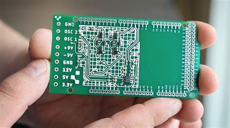
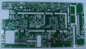
Pcb high frequency board
Design Considerations For High-Frequency PCB Boards
Designing high-frequency printed circuit boards (PCBs) necessitates a meticulous approach to ensure optimal performance and reliability. As frequencies increase, the electrical characteristics of the PCB materials and the layout become critical factors that can significantly impact signal integrity and overall functionality.
One of the primary considerations in high-frequency PCB design is the selection of appropriate materials. Traditional FR-4 substrates, commonly used in standard PCBs, may not be suitable for high-frequency applications due to their higher dielectric losses and inconsistent dielectric constant. Instead, materials such as Rogers, Teflon, or other low-loss laminates are preferred, as they offer more stable dielectric properties and lower signal attenuation.
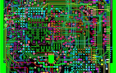
In addition to material selection, the layout of the PCB plays a crucial role in managing high-frequency signals.
Signal integrity can be compromised by factors such as crosstalk, impedance mismatches, and electromagnetic interference (EMI). To mitigate these issues, designers must carefully plan the placement and routing of traces. For instance, maintaining consistent trace widths and spacing helps to control impedance and reduce signal reflections. Furthermore, employing differential pairs for high-speed signals can minimize crosstalk and improve noise immunity.
Another important aspect of high-frequency PCB design is the management of power distribution.
Ensuring a stable power supply is essential for maintaining signal integrity and preventing noise from affecting the performance of the board. This can be achieved by using power and ground planes, which provide low-impedance paths for current flow and help to reduce voltage fluctuations. Additionally, decoupling capacitors should be strategically placed near high-frequency components to filter out noise and provide a stable voltage supply.
Thermal management is also a critical consideration in high-frequency PCB design.
High-frequency components often generate significant amounts of heat, which can affect the performance and reliability of the board if not properly managed. To address this, designers can incorporate thermal vias, heat sinks, and other cooling mechanisms to dissipate heat effectively. Moreover, selecting materials with good thermal conductivity can help to distribute heat more evenly across the board.
Signal integrity analysis is an indispensable part of the design process for high-frequency PCBs.
Simulation tools can be used to model the behavior of high-frequency signals and identify potential issues before the board is manufactured. By analyzing parameters such as signal rise time, propagation delay, and reflection coefficients, designers can make informed decisions about trace routing, layer stack-up, and component placement to optimize performance.
Furthermore, the manufacturing process itself must be considered when designing high-frequency PCBs.
Precision in etching, drilling, and layer alignment is paramount to ensure that the board meets the stringent requirements of high-frequency applications. Working closely with experienced PCB manufacturers can help to ensure that the design is translated accurately into a functional board.
In conclusion, designing high-frequency PCB boards involves a comprehensive understanding of material properties, signal integrity, power distribution, thermal management, and manufacturing processes. By carefully considering these factors and employing advanced simulation tools, designers can create high-frequency PCBs that deliver reliable performance in demanding applications. The intricate balance of these elements underscores the complexity and precision required in high-frequency PCB design, ultimately contributing to the advancement of modern electronic systems.
Material Selection For High-Frequency PCB Applications
When designing high-frequency printed circuit boards (PCBs), the selection of materials is a critical factor that significantly influences the performance, reliability, and overall functionality of the final product. High-frequency applications, typically defined as those operating above 1 GHz, demand materials with specific electrical, thermal, and mechanical properties to ensure optimal signal integrity and minimal loss. Consequently, understanding the key attributes of various materials and their impact on high-frequency PCB performance is essential for engineers and designers.
One of the primary considerations in material selection for high-frequency PCBs is the dielectric constant (Dk).
The dielectric constant measures a material’s ability to store electrical energy in an electric field. For high-frequency applications, materials with a low and stable dielectric constant are preferred, as they help maintain signal speed and reduce signal distortion. Common materials such as FR-4, which is widely used in standard PCBs, may not be suitable for high-frequency applications due to its relatively high and variable dielectric constant. Instead, materials like PTFE (Polytetrafluoroethylene), ceramic-filled laminates, and hydrocarbon-based laminates are often chosen for their low and stable Dk values.
In addition to the dielectric constant, the dissipation factor (Df) is another crucial parameter.
The dissipation factor indicates the amount of energy lost as heat within the material. For high-frequency PCBs, a low dissipation factor is essential to minimize signal loss and ensure efficient transmission of high-frequency signals. Materials such as Rogers RO3000 series and Taconic TLY series are known for their low dissipation factors, making them suitable candidates for high-frequency applications.
Thermal management is another critical aspect to consider when selecting materials for high-frequency PCBs.
High-frequency circuits often generate significant amounts of heat, which can adversely affect performance and reliability if not properly managed. Therefore, materials with good thermal conductivity are essential to dissipate heat effectively. PTFE-based laminates, for instance, offer excellent thermal properties, making them a popular choice for high-frequency applications. Additionally, materials with a low coefficient of thermal expansion (CTE) are preferred to ensure dimensional stability and prevent mechanical stress during thermal cycling.
Mechanical properties, such as rigidity and flexibility, also play a vital role in material selection
. High-frequency PCBs may be subjected to various mechanical stresses during manufacturing, assembly, and operation. Therefore, materials with adequate mechanical strength and flexibility are necessary to withstand these stresses without compromising performance. For example, ceramic-filled laminates provide excellent mechanical stability, while PTFE-based materials offer a good balance of flexibility and strength.
Furthermore, the choice of materials can impact the manufacturability and cost of high-frequency PCBs.
Advanced materials with superior electrical and thermal properties may come at a higher cost and require specialized manufacturing processes. Therefore, it is essential to strike a balance between performance requirements and cost considerations. Collaborating with experienced PCB manufacturers and material suppliers can help in selecting the most appropriate materials that meet both technical and budgetary constraints.
In conclusion, the selection of materials for high-frequency PCB applications is a multifaceted process that requires careful consideration of various electrical, thermal, and mechanical properties. By prioritizing materials with low and stable dielectric constants, low dissipation factors, good thermal conductivity, and adequate mechanical strength, designers can ensure the optimal performance and reliability of high-frequency PCBs. Balancing these technical requirements with cost considerations is crucial to achieving a successful and cost-effective design.
Signal Integrity Challenges In High-Frequency PCB Design
In the realm of high-frequency PCB design, signal integrity emerges as a paramount concern, demanding meticulous attention to detail and a profound understanding of the underlying principles. As electronic devices continue to evolve, operating at increasingly higher frequencies, the challenges associated with maintaining signal integrity become more pronounced. This necessitates a comprehensive approach to design, encompassing various factors that influence the performance and reliability of high-frequency circuits.
One of the primary challenges in high-frequency PCB design is the issue of signal loss.
At elevated frequencies, signals tend to attenuate more rapidly, primarily due to the skin effect and dielectric losses. The skin effect causes the current to concentrate near the surface of the conductor, effectively reducing the cross-sectional area available for current flow and increasing resistance. Dielectric losses, on the other hand, arise from the inherent properties of the PCB material, which can absorb and dissipate energy as heat. To mitigate these losses, designers often resort to using low-loss materials and optimizing the trace geometry to minimize resistance and maintain signal strength.
Another significant challenge is the phenomenon of signal reflection, which can severely degrade signal integrity.
Reflections occur when there is an impedance mismatch between different sections of the transmission line, causing a portion of the signal to be reflected back towards the source. This can lead to signal distortion, increased noise, and potential data errors. To address this issue, it is crucial to ensure impedance matching throughout the PCB design. This involves carefully selecting and controlling the dimensions of the traces, as well as the properties of the materials used, to achieve a consistent impedance profile.
Crosstalk is yet another critical factor that can compromise signal integrity in high-frequency PCB designs.
Crosstalk refers to the unwanted coupling of signals between adjacent traces, which can result in interference and signal degradation. The likelihood of crosstalk increases with higher frequencies and denser PCB layouts. To mitigate crosstalk, designers can employ techniques such as increasing the spacing between traces, using ground planes to provide shielding, and implementing differential signaling to reduce susceptibility to interference.
Electromagnetic interference (EMI) poses a further challenge in maintaining signal integrity.
High-frequency signals can radiate electromagnetic energy, which can interfere with other components and systems. Conversely, external sources of EMI can also affect the performance of high-frequency circuits. Effective EMI management involves a combination of design strategies, including the use of shielding, proper grounding, and the implementation of filtering techniques to suppress unwanted noise.
Thermal management is an often-overlooked aspect that can impact signal integrity in high-frequency PCB designs.
As frequencies increase, so does the power dissipation, leading to elevated temperatures that can affect the performance and reliability of the components. Ensuring adequate thermal management through the use of heat sinks, thermal vias, and appropriate PCB materials is essential to maintain signal integrity and prevent thermal-related issues.
In conclusion, the challenges associated with signal integrity in high-frequency PCB design are multifaceted and require a holistic approach to address effectively. By understanding and mitigating factors such as signal loss, reflection, crosstalk, EMI, and thermal management, designers can enhance the performance and reliability of high-frequency circuits. As technology continues to advance, the importance of maintaining signal integrity in high-frequency PCB designs will only grow, underscoring the need for ongoing research and innovation in this critical area.
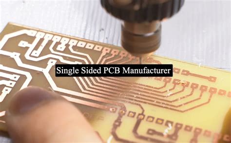
Advanced Manufacturing Techniques For High-Frequency PCBs
High-frequency printed circuit boards (PCBs) are integral to modern electronic devices, particularly in applications requiring rapid signal transmission and minimal signal loss. The advanced manufacturing techniques employed in the production of these high-frequency PCBs are crucial to ensuring their performance and reliability. One of the primary considerations in the manufacturing process is the selection of appropriate materials. High-frequency PCBs often utilize substrates such as polytetrafluoroethylene (PTFE), ceramic-filled PTFE, or other low-loss materials. These substrates are chosen for their excellent dielectric properties, which are essential for maintaining signal integrity at high frequencies. The choice of material directly impacts the board’s ability to handle high-speed signals without significant attenuation or distortion.
In addition to material selection, the precision of the manufacturing process is paramount.
Advanced photolithography techniques are employed to achieve the fine line widths and tight tolerances required for high-frequency circuits. This level of precision ensures that the impedance of the transmission lines is controlled, which is critical for minimizing signal reflection and loss. Furthermore, the use of laser direct imaging (LDI) technology allows for greater accuracy in patterning the circuit traces, thereby enhancing the overall performance of the PCB.
Another critical aspect of manufacturing high-frequency PCBs is the management of thermal properties.
High-frequency signals can generate significant heat, which, if not properly managed, can lead to performance degradation or even failure of the PCB. Advanced thermal management techniques, such as the incorporation of thermal vias and the use of heat sinks, are employed to dissipate heat effectively. These methods help maintain the operational stability of the PCB under high-frequency conditions.
Moreover, the surface finish of the PCB plays a vital role in its performance.
High-frequency PCBs often require surface finishes that provide low contact resistance and excellent solderability. Common finishes include immersion silver, immersion gold, and electroless nickel immersion gold (ENIG). These finishes not only protect the copper traces from oxidation but also ensure reliable electrical connections, which are crucial for high-frequency applications.
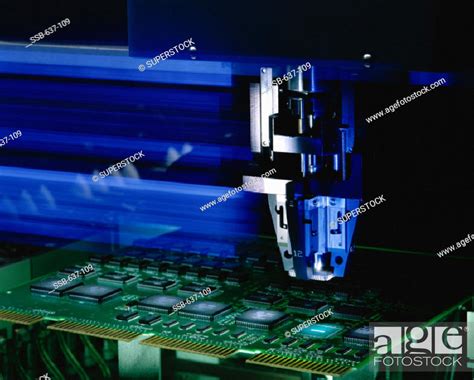
The assembly process of high-frequency PCBs also demands meticulous attention to detail.
The placement and soldering of components must be executed with high precision to avoid any misalignment or defects that could impair the board’s performance. Automated optical inspection (AOI) and X-ray inspection are commonly used to verify the accuracy of component placement and solder joints. These inspection techniques help identify and rectify any issues early in the manufacturing process, thereby enhancing the overall quality and reliability of the PCB.
Furthermore, testing and validation are essential steps in the manufacturing process of high-frequency PCBs.
Rigorous testing protocols, including time-domain reflectometry (TDR) and vector network analysis (VNA), are employed to assess the electrical performance of the PCB. These tests help ensure that the board meets the stringent requirements for high-frequency applications, providing confidence in its ability to perform reliably in demanding environments.
In conclusion, the advanced manufacturing techniques for high-frequency PCBs encompass a range of critical processes, from material selection and precision photolithography to thermal management and rigorous testing. Each step is meticulously executed to ensure that the final product meets the high standards required for modern electronic applications. By leveraging these advanced techniques, manufacturers can produce high-frequency PCBs that deliver exceptional performance and reliability, thereby supporting the ever-evolving demands of the electronics industry.