PCB Impedance Control: A Comprehensive Guide
Introduction to PCB Impedance Control
Printed Circuit Board (PCB) impedance control is a critical aspect of modern electronics design, particularly for high-speed digital circuits and high-frequency analog applications. As signal frequencies continue to increase in today’s electronic devices, maintaining controlled impedance throughout PCB traces has become essential for ensuring signal integrity and proper circuit operation.
Impedance control refers to the practice of designing PCB traces to have a specific characteristic impedance, typically matching the impedance of connected components and transmission lines. This matching prevents signal reflections that can cause distortion, ringing, and other signal integrity issues that degrade system performance.
The Importance of Impedance Control
Signal Integrity Considerations
In high-speed digital systems (generally considered above 50MHz), PCB traces behave less like simple conductors and more like transmission lines. When the propagation time of a signal becomes significant compared to its rise time, impedance mismatches can lead to:
- Signal reflections that cause overshoot, undershoot, and ringing
- Intersymbol interference in digital systems
- Increased electromagnetic interference (EMI)
- Reduced noise margins and potential logic errors
Common Applications Requiring Impedance Control
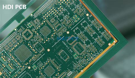
- High-speed digital interfaces (DDR memory, PCI Express, USB 3.0+)
- RF circuits and wireless communications
- High-frequency analog circuits
- Differential signaling systems (LVDS, HDMI)
- High-speed networking equipment
Fundamental Concepts of Transmission Lines
To properly understand impedance control, we must first examine some fundamental transmission line concepts:
Characteristic Impedance (Z₀)
The characteristic impedance of a transmission line is determined by its physical geometry and material properties, not by its length. For PCB traces, the key factors affecting impedance are:
- Trace width (W)
- Trace thickness (T)
- Dielectric height (H) between trace and reference plane
- Dielectric constant (εᵣ or Dk) of the PCB material
- Presence and proximity of adjacent traces
Common Impedance Values
Typical impedance values used in PCB design include:
- Single-ended traces: 50Ω (common for RF), 75Ω (video)
- Differential pairs: 90Ω (USB), 100Ω (Ethernet, PCIe)
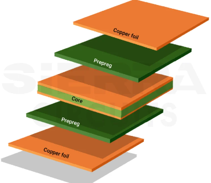
PCB Stackup Design for Impedance Control
Proper PCB stackup design is foundational for achieving controlled impedance. Key considerations include:
Layer Arrangement
- Signal layers should be adjacent to solid reference planes (power or ground)
- Maintain consistent dielectric thicknesses for predictable impedance
- Consider microstrip vs. stripline configurations
Material Selection
- FR-4 is common but has εᵣ that varies with frequency (~4.2-4.8)
- High-frequency laminates (Rogers, Isola) offer more stable εᵣ
- Consider dielectric loss tangent for very high frequency applications
Impedance Calculation Methods
Microstrip Transmission Lines
Microstrip refers to traces on an external layer with a single reference plane. The simplified impedance formula is:
Z₀ ≈ [87/√(εᵣ+1.41)] × ln[5.98H/(0.8W+T)]
Where:
- Z₀: Characteristic impedance (Ω)
- εᵣ: Dielectric constant
- H: Dielectric height (mm)
- W: Trace width (mm)
- T: Trace thickness (mm)
Stripline Transmission Lines
Stripline refers to traces embedded between two reference planes. The simplified impedance formula is:
Z₀ ≈ [60/√εᵣ] × ln[4H/(0.67π(0.8W+T))]
Differential Pairs
Differential impedance depends on:
- The impedance of each single-ended trace
- The spacing (S) between the pair
- The coupling between traces
Practical Design Considerations
Trace Geometry
- Maintain consistent trace widths (avoid neck-downs)
- Minimize use of vias in impedance-controlled traces
- Keep bends at ≥ 45° angles or use curved traces
- Maintain proper spacing to other traces
Manufacturing Tolerances
Typical PCB manufacturing tolerances that affect impedance:
- Trace width: ±10-20%
- Dielectric thickness: ±10%
- Copper thickness: ±1/2 oz variation
- Dielectric constant: ±5-10%
Designers should work with their PCB manufacturer to understand specific capabilities and adjust designs accordingly.
Impedance Matching Techniques
Source Termination
Adding series resistance at the driver equal to:
R = Z₀ – R_driver
End Termination
Parallel termination at the receiver with:
R = Z₀
AC Termination
Capacitive termination that only affects high-frequency components
Measurement and Verification
Time Domain Reflectometry (TDR)
The gold standard for impedance measurement, TDR sends a fast edge signal and measures reflections to determine impedance variations along the trace.
Network Analysis
Vector Network Analyzers (VNA) can measure impedance in the frequency domain, useful for RF applications.
Manufacturing Testing
Many PCB manufacturers perform impedance testing on test coupons that accompany production boards.
Common Challenges and Solutions
Impedance Discontinuities
Caused by:
- Vias
- Connectors
- Layer changes
- Test points
Solutions include:
- Via stitching
- Return path vias near signal vias
- Minimizing layer transitions
Crosstalk Between Traces
Mitigated by:
- Proper spacing (3× dielectric height is a good rule)
- Guard traces
- Orthogonal routing on adjacent layers
Advanced Topics
Frequency-Dependent Effects
At very high frequencies (>10GHz):
- Skin effect increases resistance
- Dielectric losses become significant
- Surface roughness affects impedance
3D Field Solvers
For critical applications, 3D electromagnetic field solvers provide the most accurate impedance calculations by considering:
- Exact trace geometries
- Material properties
- Surrounding structures
Conclusion
PCB impedance control is an essential discipline in modern electronics design, particularly as signal speeds continue to increase. By understanding transmission line theory, carefully designing PCB stackups, calculating appropriate trace geometries, and working closely with manufacturing partners, designers can achieve the impedance control needed for reliable high-speed operation. While the concepts can be complex, the tools and techniques for impedance control are well-established and accessible to PCB designers at all levels. As technology advances, impedance control will remain a critical factor in ensuring signal integrity and system performance across a wide range of electronic applications.
Future Trends
Looking ahead, we can expect:
- Tighter impedance tolerances as speeds increase
- More sophisticated materials with stable εᵣ over wider frequency ranges
- Improved modeling tools incorporating more physical effects
- Automated impedance verification during manufacturing
By staying current with these developments, PCB designers can continue to meet the challenges of ever-faster electronic systems.