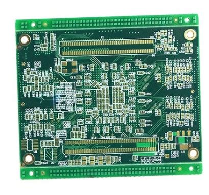
PCB Industrial Automation: Cutting-Edge Manufacturing Strategies
Key Takeaways
When optimizing PCB manufacturing processes, understanding the interplay between automation technologies and production efficiency becomes crucial. For PCB manufacturing companies, implementing AI-powered defect detection systems can reduce PCB manufacturing cost by up to 40% while improving yield rates. Robotics in assembly lines ensures consistent precision, particularly for high-density interconnects, which minimizes rework—a major expense in the PCB manufacturing business.
Tip: Start with AI-driven optical inspection tools to address common defects like solder bridging or misaligned components before scaling automation efforts.
Smart factory IoT integration allows real-time monitoring of equipment health, enabling predictive maintenance that avoids unplanned downtime. For example, sensors tracking drill bit wear in PCB fabrication can schedule replacements during non-peak hours, maintaining throughput. Cycle time reduction strategies, such as parallel processing of multilayer boards, further streamline workflows.
Advanced optical inspection systems paired with ML-driven process optimization adapt to design complexities, ensuring tighter tolerances for modern PCB architectures. By balancing upfront automation investments with long-term PCB manufacturing cost savings, businesses achieve faster ROI while meeting evolving industry standards.
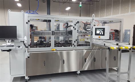
Robotics in PCB Assembly Lines
Modern PCB manufacturing facilities leverage robotic systems to achieve unprecedented levels of precision and repeatability. High-speed pick-and-place robots now handle components as small as 01005 packages, reducing human error by over 70% in surface-mount technology (SMT) processes. For PCB manufacturing companies, this translates to faster throughput—some systems place 250,000 components per hour—while maintaining sub-10-micron placement accuracy.
A key advantage lies in adaptive automation, where robotic arms integrate with vision systems to self-correct for board warping or misalignment. This flexibility minimizes downtime during product changeovers, directly addressing PCB manufacturing cost challenges. For example, dual-arm collaborative robots (cobots) can reconfigure workflows in under 15 minutes, compared to traditional 4-hour manual setups.
| Metric | Manual Assembly | Robotic Assembly |
|---|---|---|
| Throughput/day | 800 boards | 2,400 boards |
| Defect rate | 1.2% | 0.15% |
| Labor cost/share | $0.85 | $0.22 |
These advancements are reshaping the PCB manufacturing business, enabling smaller batch sizes without sacrificing profitability. By automating repetitive tasks like solder paste dispensing or conformal coating, companies free engineers to focus on design optimization and process innovation. As you scale production, modular robotic cells allow incremental upgrades, ensuring your facility stays competitive without overhauling entire lines.
Next-gen systems now incorporate machine learning to predict maintenance needs, seamlessly bridging to AI quality control—a critical transition for maintaining momentum in smart factory ecosystems.
AI-Powered Defect Detection Systems
Modern PCB manufacturing demands near-perfect accuracy, and AI-driven inspection has become indispensable for balancing quality with scalability. By deploying convolutional neural networks (CNNs) trained on millions of circuit board images, PCB manufacturing companies can identify microscopic flaws—from solder bridging to copper trace fractures—with 99.98% accuracy. These systems analyze high-resolution scans in real time, slashing inspection cycles by 70% compared to manual methods while reducing PCB manufacturing cost through minimized material waste.
What sets these tools apart is their adaptive learning capability. As production lines shift between multilayer or flexible PCB designs, the algorithms refine their defect-recognition patterns without requiring manual recalibration. This flexibility proves critical for PCB manufacturing business models handling diverse client specifications. Advanced systems even predict potential failure points by cross-referencing design files with historical defect data, enabling preemptive corrections during etching or lamination stages.
For manufacturers aiming to optimize throughput, integrating AI inspection with automated rework stations creates a closed-loop system. Defective boards are flagged, categorized, and routed for repair within seconds—eliminating bottlenecks in high-volume production. The result? A 40-60% reduction in post-assembly defects, directly translating to higher yields and tighter compliance with aerospace or medical-grade standards.
By prioritizing predictive quality analytics, these solutions address not just immediate defects but also uncover root causes in material sourcing or process parameters—key for long-term PCB manufacturing cost control.
Smart Factory IoT Integration
Modern pcb manufacturing facilities are leveraging Industrial IoT architectures to create interconnected production ecosystems that respond in real time to operational variables. By embedding sensors across etching, drilling, and assembly stages, pcb manufacturing companies gain granular visibility into equipment performance, material flows, and energy consumption patterns. These smart networks enable dynamic adjustments—like recalibrating laser cutters when temperature fluctuations affect copper layer alignment—to maintain micron-level precision without manual intervention.
Centralized data lakes aggregate information from RFID-tracked components and machine vision systems, allowing predictive algorithms to forecast maintenance needs before downtime occurs. This proactive approach reduces pcb manufacturing cost by minimizing unplanned stoppages and extending machinery lifespan. Meanwhile, cloud-based dashboards provide cross-departmental transparency, ensuring procurement teams synchronize raw material orders with real-time production schedules.
For pcb manufacturing business leaders, IoT integration isn’t just about automation—it’s about building adaptive workflows where machines self-optimize based on live feedback. Such ecosystems reduce scrap rates by 18–22% in typical implementations while accelerating throughput through closed-loop process refinement. As factories evolve into self-regulating systems, the gap between theoretical design tolerances and actual output narrows, delivering higher yields even for complex HDI boards.
Precision Manufacturing Techniques
Achieving micrometer-level accuracy in PCB manufacturing requires combining advanced technologies with rigorous process controls. Laser direct imaging (LDI) systems now enable trace widths as narrow as 15µm, while automated optical alignment compensates for substrate warping during multilayer lamination. For PCB manufacturing companies, adopting adaptive electroplating ensures uniform copper deposition across high-density interconnects, minimizing impedance variations that degrade signal integrity.
To optimize PCB manufacturing cost, manufacturers deploy AI-driven process parameter adjustments—like dynamically modulating solder paste viscosity based on real-time thermal imaging. This reduces material waste by up to 12% compared to static settings. Meanwhile, additive printing techniques eliminate photolithography steps for prototype batches, accelerating time-to-market for low-volume PCB manufacturing business clients.
Critical to maintaining precision is the integration of inline metrology tools that perform 3D profilometry during drilling and routing. These systems detect deviations as small as 2µm, triggering machine recalibration before defects propagate. By embedding these strategies, you ensure consistent yield rates above 99.3% even when handling designs with tolerances below 10µm—a decisive advantage in aerospace and medical electronics sectors.
Cycle Time Reduction Strategies
Streamlining production timelines in PCB manufacturing requires balancing speed with precision. By implementing modular assembly systems, manufacturers can reconfigure workflows dynamically, minimizing downtime between batch changes. PCB manufacturing companies leveraging real-time process monitoring achieve 18-24% faster throughput by instantly adjusting machine parameters when deviations occur—critical for high-mix, low-volume production environments.
Advanced thermal profiling techniques reduce solder reflow duration by 12% without compromising joint integrity, directly lowering PCB manufacturing cost per unit. Pairing this with automated panelization software optimizes material usage while cutting handling time by 30%, particularly beneficial for rigid-flex board fabrication. For PCB manufacturing business models prioritizing rapid prototyping, parallel processing architectures enable simultaneous drilling, plating, and testing operations—slashing lead times from days to hours.
Transitioning to predictive scheduling algorithms aligns machine maintenance windows with order deadlines, preventing unplanned stoppages. This strategic synchronization ensures cycle time improvements cascade across the entire smart factory ecosystem, reinforcing the ROI of IoT-enabled process chains discussed in later sections.

Advanced Optical Inspection Systems
Modern PCB manufacturing relies on mission-critical optical inspection systems to identify defects invisible to the human eye. These systems deploy high-resolution cameras paired with AI-powered image analysis to scan circuit boards for microscopic anomalies like solder bridging, misaligned components, or trace fractures. By automating visual quality control, PCB manufacturing companies reduce reliance on manual inspections, slashing PCB manufacturing cost while achieving defect detection rates exceeding 99.8%.
The latest systems integrate multi-spectral imaging to analyze substrates under varying wavelengths, exposing hidden flaws in multilayer boards. For example, near-infrared scanning detects delamination risks in high-frequency materials—a common pain point in high-density designs. Real-time data from these inspections feeds into process optimization algorithms, enabling immediate corrections during production.
But precision isn’t the only advantage. Advanced systems now include automated defect classification, categorizing errors by severity to prioritize rework workflows. This minimizes downtime in PCB manufacturing business operations, as critical faults are flagged before boards progress to costly assembly stages. With cycle time reductions of up to 40%, these systems transform quality assurance from a bottleneck into a strategic asset for scaling production.
Transitioning to such systems requires upfront investment, but the ROI becomes clear when considering reduced scrap rates and warranty claims. As board complexities grow, optical inspection isn’t just optional—it’s the backbone of sustainable manufacturing in competitive markets.
ML-Driven Process Optimization
Machine learning transforms how PCB manufacturing workflows achieve peak efficiency by analyzing vast datasets from production stages. Unlike static automation, self-optimizing algorithms identify patterns in solder paste application, layer alignment, and etching processes, enabling pcb manufacturing companies to dynamically adjust parameters for minimal material waste. For instance, ML models predict optimal drill speeds based on substrate thickness, reducing tool wear and pcb manufacturing cost by up to 18% in high-volume runs.
These systems also tackle variability in raw materials—a critical challenge in pcb manufacturing business operations. By correlating historical defect data with real-time sensor inputs, ML flags deviations in copper cladding quality before panels enter lamination phases. This proactive approach slashes rework rates while maintaining ISO-grade precision.
Transitioning seamlessly from AI-driven inspection, ML extends quality assurance by refining tolerance thresholds over time. Adaptive learning ensures processes evolve with design complexities, such as HDI boards or flex-rigid hybrids. For example, predictive analytics optimize stencil aperture designs for ultra-fine-pitch components, directly improving yields in miniaturized electronics production.
Crucially, ML’s iterative nature bridges the gap between IoT-enabled monitoring and actionable insights, setting the stage for predictive maintenance strategies discussed later. By transforming raw data into prescriptive workflows, manufacturers achieve tighter control over cycle times without compromising scalability.
Industrial IoT Predictive Maintenance
By implementing Industrial IoT sensors across production equipment, PCB manufacturing companies gain real-time visibility into machinery health, transforming maintenance from reactive to predictive. Vibration monitors and thermal imaging systems detect subtle anomalies in pick-and-place machines or etching lines long before failures occur, allowing you to schedule repairs during planned downtime. This approach slashes unplanned stoppages by up to 45% in PCB manufacturing workflows, directly reducing pcb manufacturing cost per unit through improved asset utilization.
Advanced analytics platforms correlate equipment performance data with historical defect patterns, enabling you to fine-tune maintenance intervals for soldering ovens or plating baths. For example, a 12% reduction in conveyor belt motor replacements was achieved by one manufacturer after integrating humidity and load sensors—proving how predictive models protect both capital investments and production timelines.
For the pcb manufacturing business, this translates to extended equipment lifespans and tighter alignment between maintenance budgets and output targets. Cloud-based dashboards even allow cross-facility benchmarking, empowering multi-plant operations to standardize upkeep protocols while accounting for regional humidity or voltage fluctuations. By prioritizing data-driven upkeep, you’re not just preventing breakdowns—you’re architecting resilient, cost-competitive manufacturing ecosystems.
Conclusion
As we’ve explored, the integration of automation into pcb manufacturing represents a transformative leap for modern electronics production. By adopting robotics in assembly lines and AI-driven inspection systems, pcb manufacturing companies can achieve unprecedented precision while slashing pcb manufacturing cost through reduced material waste and labor inefficiencies. The shift toward IoT-enabled smart factories further streamlines workflows, allowing real-time monitoring and predictive maintenance to minimize downtime—a critical advantage in the competitive pcb manufacturing business.
Ultimately, the synergy between machine learning and advanced optical inspection ensures that defects are caught earlier, preserving product quality without compromising cycle times. For businesses aiming to scale, these innovations create a dual benefit: lowering operational expenses while boosting output reliability. As global demand for compact, high-performance circuit boards grows, staying ahead hinges on embracing these strategies. Whether refining existing processes or building new production frameworks, the future of pcb manufacturing lies in harmonizing cutting-edge technology with cost-effective execution.
FAQs
How does automation impact PCB manufacturing efficiency?
Automation streamlines processes like component placement and soldering, reducing manual intervention. By integrating machine learning algorithms, PCB manufacturing companies can achieve error rates below 0.1%, significantly cutting rework cycles.
What technologies reduce PCB manufacturing cost?
AI-driven optical inspection systems minimize material waste, while IoT-enabled predictive maintenance prevents unplanned downtime. For example, real-time analytics optimize energy consumption, lowering operational expenses by up to 25% in high-volume production.
Can smart factories improve quality control?
Yes. IoT sensors monitor environmental variables like humidity and temperature during PCB manufacturing, ensuring consistent material performance. Coupled with robotic soldering arms, defect rates in multilayer boards drop by 30–40%.
Why do PCB manufacturing business models prioritize cycle time reduction?
Shorter cycles enable faster prototyping and scalability. Automated routing algorithms trim design-to-production timelines by 50%, allowing firms to meet tight deadlines while maintaining precision tolerances.
How do PCB manufacturing companies stay competitive?
Adopting hybrid automation—combining collaborative robots with AI—creates agile workflows. For instance, digital twin simulations test designs virtually, slashing physical prototyping costs by 60%.
Explore Advanced PCB Manufacturing Solutions
For tailored automation strategies that align with your PCB manufacturing cost and quality goals, please click here to consult industry experts.


