PCB Inner Layer Circuit Manufacturing Process and Key Considerations
Introduction
Printed Circuit Boards (PCBs) are essential components in modern electronics, providing mechanical support and electrical connections for electronic components. The inner layers of multilayer PCBs are critical for signal integrity and power distribution. This article explores the manufacturing process of PCB inner layer circuits and highlights key considerations to ensure quality and reliability.
1. PCB Inner Layer Circuit Manufacturing Process
The production of inner layer circuits involves several precise steps, including material preparation, imaging, etching, and inspection. Below is a detailed breakdown of the process.
1.1 Material Preparation
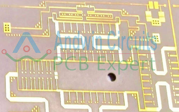
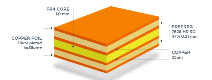
The inner layer of a PCB typically consists of a copper-clad laminate (CCL), which is a dielectric substrate (e.g., FR-4) coated with copper foil.
- Substrate Selection: The dielectric material must meet thermal, mechanical, and electrical requirements. FR-4 is commonly used due to its flame resistance and stability.
- Copper Thickness: The copper foil thickness (e.g., ½ oz, 1 oz, 2 oz) depends on current-carrying requirements.
1.2 Cleaning and Surface Treatment
Before patterning, the copper surface must be cleaned to remove contaminants (dust, oxides, oils).
- Mechanical Scrubbing: Uses abrasive brushes or pumice to roughen the surface for better adhesion.
- Chemical Cleaning: Acid or alkaline solutions remove organic residues.
1.3 Photoresist Application
A photosensitive film (photoresist) is applied to the copper surface to transfer the circuit pattern.
- Dry Film Photoresist: A dry film is laminated onto the copper using heat and pressure.
- Liquid Photoresist: Applied via spray or spin coating for high-resolution circuits.
1.4 Exposure and Development
The photoresist is exposed to UV light through a photomask (film with the circuit pattern).
- Exposure: UV light hardens the exposed photoresist (for negative resist) or softens it (for positive resist).
- Development: A chemical solution removes the unexposed resist, revealing the copper areas to be etched.
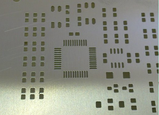
1.5 Etching
The unwanted copper is removed using an etching solution, leaving only the desired circuit traces.
- Etching Chemicals: Ferric chloride (FeCl₃) or ammonium persulfate is commonly used.
- Etching Process: The board is sprayed or immersed in the etchant, dissolving unprotected copper.
1.6 Stripping and Cleaning
After etching, the remaining photoresist is stripped, and the board is cleaned.
- Photoresist Removal: Alkaline solutions dissolve the resist.
- Final Cleaning: Ensures no residues remain before further processing.
1.7 Automated Optical Inspection (AOI)
The inner layer undergoes AOI to detect defects such as shorts, opens, or etching errors.
- High-Resolution Cameras: Scan the board and compare it to the design file.
- Defect Marking: Faulty boards are flagged for rework or rejection.
1.8 Oxide Treatment (Optional)
For multilayer PCBs, a brown or black oxide treatment enhances adhesion between layers.
- Chemical Oxidation: Creates a micro-roughened surface for better bonding during lamination.
1.9 Lamination (For Multilayer PCBs)
Inner layers are stacked with prepreg (pre-impregnated dielectric) and outer copper foils, then pressed under heat and pressure to form a solid board.
2. Key Considerations in Inner Layer Manufacturing
To ensure high-quality inner layers, manufacturers must address several critical factors.
2.1 Material Selection
- Dielectric Properties: The substrate must have stable dielectric constant (Dk) and loss tangent (Df) for signal integrity.
- Copper Quality: Low-profile copper foils reduce signal loss in high-frequency applications.
2.2 Photoresist and Exposure Control
- Resolution: Fine-line circuits require high-resolution photoresist and precise exposure.
- Alignment: Misalignment between layers can cause impedance mismatches.
2.3 Etching Uniformity
- Over-Etching/Under-Etching: Can lead to trace width deviations or incomplete copper removal.
- Etch Factor: The ratio of vertical to lateral etching affects trace geometry.
2.4 Dimensional Stability
- Thermal Expansion: Substrate materials must resist warping during lamination.
- Registration Accuracy: Inner layers must align precisely to avoid layer-to-layer misregistration.
2.5 Defect Prevention
- Contamination Control: Dust or residues can cause shorts or weak adhesion.
- AOI Optimization: High-sensitivity inspection reduces escape rates for defects.
2.6 Environmental and Safety Considerations
- Chemical Handling: Etchants and developers require proper disposal.
- Worker Safety: Ventilation and protective equipment are essential.
3. Common Defects and Troubleshooting
| Defect | Possible Causes | Solutions |
|---|---|---|
| Short Circuits | Overexposure, under-etching | Adjust exposure time, improve etching control |
| Open Circuits | Over-etching, resist peeling | Optimize etchant concentration, improve resist adhesion |
| Poor Adhesion | Contaminated surface, incorrect lamination | Enhance cleaning, adjust lamination parameters |
| Misregistration | Material expansion, alignment errors | Use dimensionally stable substrates, improve alignment systems |
4. Conclusion
The manufacturing of PCB inner layer circuits requires precision at every stage, from material selection to etching and inspection. By understanding the process and adhering to best practices, manufacturers can produce high-quality, reliable PCBs for advanced electronic applications. Continuous improvements in imaging, etching, and inspection technologies further enhance yield and performance.
Future Trends
- Laser Direct Imaging (LDI): Improves resolution for ultra-fine traces.
- Advanced Materials: Low-loss dielectrics for high-speed PCBs.
- Automation & AI: Enhanced defect detection and process control.
By following these guidelines, PCB manufacturers can optimize inner layer production and meet the growing demands of modern electronics.