PCB Inner Layer Design for Manufacturability
Join the Discussion Group
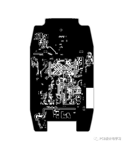
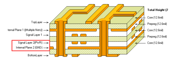
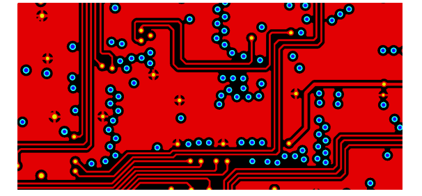
When a PCB engineer lays out a product, it’s not just about layout and routing; the design of the inner power and ground planes is also crucial. When designing inner layers, not only power integrity, signal integrity, and electromagnetic compatibility must be considered, but also design, manufacturing, and performance factors. The difference between inner and outer PCB layers is that outer layers are used for routing and soldering components, while inner layers are designed for power and ground planes. These layers are only used in multi-layer boards and are primarily used for routing power and ground traces. These layers are referred to as two-layer, four-layer, and six-layer boards, typically referring to the number of signal layers and internal power and ground planes.
Inner Layer Design
Design a ground plane below critical signals such as high-speed, test, and high-frequency signals to minimize signal loop paths and radiation.
When designing high-speed circuits, it’s crucial to consider how to manage power supply radiation and overall system interference. Generally, the power plane area should be smaller than the ground plane area to provide shielding. Generally, the power plane should be set back twice the dielectric thickness of the ground plane.
Layer Stacking Planning
The power plane should be adjacent to the corresponding ground plane. This creates a coupling capacitor that works together with the decoupling capacitors on the PCB to reduce the impedance of the power plane and achieve a wide filtering effect.
Reference Plane
02
The selection of a reference plane is very important. In theory, either the power plane or the ground plane can serve as a reference plane, but the ground plane can generally be connected to ground and provides much better shielding than the power plane, so the ground plane is generally preferred as the reference plane.
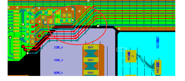
Signal lines should not cross zones.
03
Critical signals on two adjacent layers should not cross partitions. Otherwise, large signal loops will form, resulting in strong radiation and coupling.
Power and Ground Trace Planning
04
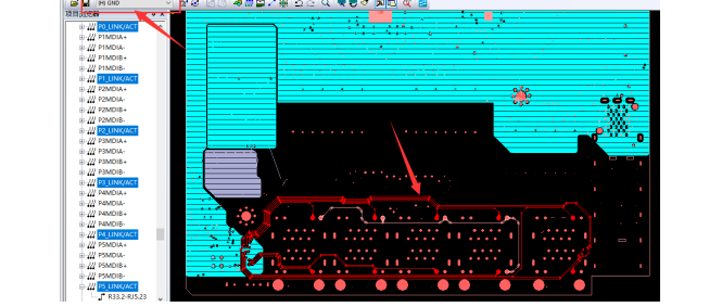
To maintain the integrity of the ground plane, routing should not occur within it. If signal trace density is too high, consider routing traces along the edge of the power plane.
Inner Layer Manufacturing
Due to the complex PCB manufacturing process, inner layer manufacturing is only one part of the equation. When producing inner layer boards, it’s also important to consider how other process steps can impact the manufacturing capabilities of the inner layers. For example, press-fit tolerances and drilling tolerances can affect the quality and yield of the inner layers.
PCBs can be categorized as single-sided, double-sided, or multi-layer boards, depending on the number of layers. These three types of boards also have significantly different manufacturing processes. Multi-layer boards, in particular, have a significantly more complex manufacturing process than single-sided or double-sided boards. Therefore, when designing a multi-layer board, it’s important to consider the complex manufacturing process and consider design for manufacturability (DFM).
1 Deleting Independent Pads
Independent pads are non-functional pads on inner layers that are not connected to any nets. These pads are removed during the PCB manufacturing process. While removing these pads has no impact on the product’s design functionality, it can actually affect quality and production efficiency during manufacturing.
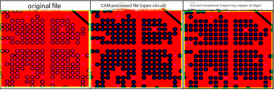
2 Inner Layer BGA Area
BGA devices are relatively small and have numerous pins, resulting in dense fan-out vias. During manufacturing, a certain distance must be maintained between the drilled holes and the traces and copper foil, otherwise shorts may occur during the press-fit and drilling processes. When maintaining a certain distance between the drilled holes and the copper foil and traces, the copper between the holes cannot be retained, resulting in open circuits. Therefore, when CAM engineers work on the BGA area, they must be aware of any copper opens between the holes and fill in the copper bridges to ensure consistent network connectivity after production.
3 Inner Layer Design Anomaly
All vias in the inner layer negative sheet have via rings. When converted to the positive sheet, these vias are completely disconnected from the copper sheet, effectively isolating the inner layer. Complete isolation means the inner layer serves no purpose, and it can be omitted. If this issue is encountered during production, the design engineer will be contacted to determine if there is a design anomaly, or if the inner layer copper sheet lacks a network, leading to complete isolation.

4 Inner Layer Negative Sheet Bottleneck
When designing the power and ground layers in the inner layer, dense vias can create a bottleneck in network connectivity. If the copper bridge width for the power network is insufficient, the current cannot flow properly, resulting in board burnout. Some bottlenecks can even result in open circuits, leading to product design failure.