PCB Inspection: Techniques, Challenges, and Future Trends
Introduction
Printed Circuit Boards (PCBs) are the backbone of modern electronics, serving as the foundation for nearly all electronic devices. As PCBs become more complex with higher component density and finer traces, ensuring their quality through inspection has become critical. PCB inspection is a vital step in the manufacturing process, helping to detect defects early, reduce production costs, and improve reliability.
This article explores various PCB inspection techniques, their advantages and limitations, common challenges, and emerging trends in automated inspection technologies.
1. Importance of PCB Inspection
PCB inspection ensures that manufactured boards meet design specifications and function correctly. Defects such as short circuits, open traces, misaligned components, or soldering issues can lead to device failure. Inspection helps:
- Improve yield rates by identifying defects early in production.
- Reduce costs by preventing faulty PCBs from reaching later assembly stages.
- Enhance reliability by ensuring compliance with industry standards (e.g., IPC-A-610).
- Support miniaturization as PCBs become smaller and more complex.
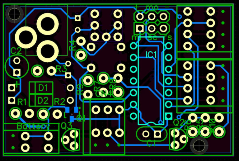
2. Types of PCB Inspection Techniques
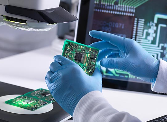
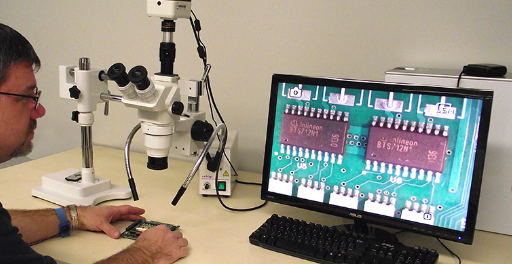
2.1 Manual Visual Inspection (MVI)
MVI is the simplest form of inspection, where technicians examine PCBs under magnification for visible defects.
Advantages:
- Low initial cost (no specialized equipment needed).
- Effective for large components and obvious defects.
Limitations:
- Prone to human error and fatigue.
- Inconsistent across different inspectors.
- Not suitable for high-density or micro-scale PCBs.
2.2 Automated Optical Inspection (AOI)
AOI uses high-resolution cameras and image processing software to detect defects by comparing PCB images against a reference design.
Advantages:
- Fast and repeatable.
- Detects common defects (solder bridges, missing components, misalignment).
- Works well for surface-mount technology (SMT) inspection.
Limitations:
- Limited ability to inspect hidden solder joints (e.g., under BGA components).
- Requires proper lighting and calibration.
2.3 X-Ray Inspection (AXI)
Automated X-ray inspection (AXI) is used for examining hidden solder joints, such as those in Ball Grid Arrays (BGAs) and through-hole components.
Advantages:
- Detects defects invisible to optical methods (voids, insufficient solder).
- Essential for complex, high-density PCBs.
Limitations:
- Expensive equipment and slower than AOI.
- Requires skilled operators for interpretation.
2.4 In-Circuit Testing (ICT)
ICT uses electrical probes to test individual components and connections on a powered PCB.
Advantages:
- Highly accurate for detecting electrical faults (shorts, opens, wrong components).
- Provides functional testing of circuits.
Limitations:
- Requires custom test fixtures, increasing cost.
- Less effective for mechanical defects (e.g., solder cracks).
2.5 Flying Probe Testing
A more flexible alternative to ICT, flying probe testers use movable probes to check PCBs without needing a dedicated fixture.
Advantages:
- No fixture costs, ideal for low-volume production.
- Can test high-density PCBs effectively.
Limitations:
- Slower than ICT for large batches.
- Limited power-up testing capabilities.
2.6 3D SPI (Solder Paste Inspection)
3D SPI systems measure solder paste deposition before component placement, ensuring proper volume and alignment.
Advantages:
- Prevents soldering defects early in assembly.
- Reduces rework costs.
Limitations:
- Only applicable at the solder paste stage.
3. Common PCB Defects Detected by Inspection
PCB inspection methods target various defects, including:
- Solder Bridges – Unintended connections between pads.
- Open Circuits – Broken traces or insufficient solder.
- Component Misalignment – Incorrectly placed parts.
- Tombstoning – One end of a component lifts during soldering.
- Insufficient/Excess Solder – Affects electrical and mechanical reliability.
- Voids in Solder Joints – Air pockets weakening connections (detected via X-ray).
4. Challenges in PCB Inspection
Despite advancements, PCB inspection faces several challenges:
- High-Density Designs – Smaller components and tighter spacing make defects harder to detect.
- Flex and Rigid-Flex PCBs – Non-flat surfaces complicate optical inspection.
- False Positives/Negatives – Overly sensitive inspection systems may flag acceptable variations as defects.
- Cost vs. Accuracy Trade-off – High-end inspection systems (e.g., AXI) are expensive but necessary for advanced PCBs.
- Speed Constraints – Faster production lines require real-time inspection without bottlenecks.
5. Future Trends in PCB Inspection
Emerging technologies are transforming PCB inspection:
5.1 AI and Machine Learning
- AI-powered vision systems improve defect recognition and reduce false positives.
- Deep learning models can adapt to new PCB designs without manual reprogramming.
5.2 3D AOI and Enhanced X-Ray
- Higher-resolution 3D imaging provides better defect analysis.
- Computed Tomography (CT) scans offer detailed internal inspections.
5.3 Automated Defect Classification (ADC)
- AI-driven classification speeds up defect analysis and root cause identification.
5.4 In-Line and Real-Time Inspection
- Integration with production lines allows instant feedback and process adjustments.
5.5 IoT and Industry 4.0 Integration
- Smart factories use inspection data for predictive maintenance and process optimization.
6. Conclusion
PCB inspection is a critical step in ensuring the quality and reliability of electronic products. While traditional methods like MVI and AOI remain useful, advanced techniques such as AXI, 3D SPI, and AI-driven inspection are becoming essential for modern, high-density PCBs.
The future of PCB inspection lies in automation, AI, and real-time analytics, enabling faster, more accurate defect detection while reducing costs. As PCB technology evolves, inspection methods must continue advancing to meet the demands of next-generation electronics.
By adopting the right inspection strategies, manufacturers can improve yields, reduce waste, and deliver higher-quality products to the market.