PCB interference suppression design, you must know these 47 principles
Radiation generation
Current causes radiation, not voltage, static charges produce electrostatic fields, constant currents produce magnetic fields, and time-varying currents produce both electric and magnetic fields. There are common mode current and differential mode current in any circuit. The differential mode signal carries data or useful signal, and the common mode signal is the negative effect of the differential mode mode.
Differential mode current
Equal in size and opposite in direction (phase). Due to the distributed capacitance and inductance of the traces, discontinuous signal trace impedance, and the signal return path flowing through unexpected paths, the differential mode current will be converted into a common mode current.
Common mode current
The sizes are not necessarily equal, but the directions (phases) are the same. The external interference from equipment is mostly common mode, and differential mode interference also exists, but the intensity of common mode interference is often several orders of magnitude greater than the intensity of differential mode. External interference is mostly common mode interference. Common mode interference itself generally does not cause harm to the equipment, but if the common mode interference turns into differential mode interference, it will be serious because the useful signals are all differential mode signals. The magnetic field of the differential mode current is mainly concentrated in the loop area formed by the differential mode current. Outside the loop area, the magnetic lines of force will cancel each other. The magnetic field of the common mode current is outside the loop area, and the magnetic field generated by the common mode current has the same direction. Many EMC designs of PCBs follow the above theory.
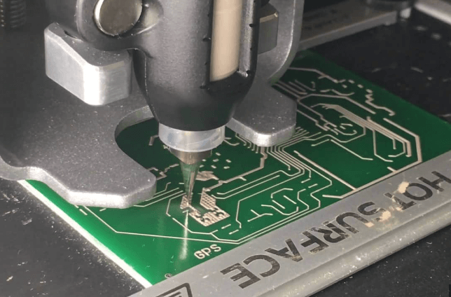
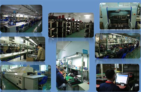
GET PCB MANUFACTURING AND ASSEMBLY QUOTE NOW!
Ways to suppress interference on PCB boards include:
1. Reduce the differential mode signal loop area.
2. Reduce high-frequency noise backflow (filtering, isolation and matching).
3. Reduce the common mode voltage (grounding design). 47 principles of high-speed PCB EMC design
GET PCB AND ASSEMBLY SERVICE QUOTE NOW!
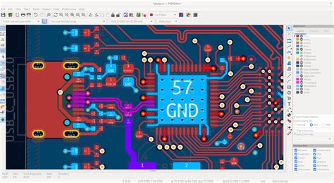
Summary of PCB design principles
Principle 1: If the PCB clock frequency exceeds 5MHZ or the signal rise time is less than 5ns, a multi-layer board design is generally required.
Reason: The signal loop area can be well controlled by using multi-layer board design.
Principle 2: For multi-layer boards, key wiring layers (layers where clock lines, busses, interface signal lines, RF lines, reset signal lines, chip select signal lines, and various control signal lines are located) should be adjacent to the complete ground plane. Preferably between two ground planes.
Reason: Key signal lines are generally strong radiation or extremely sensitive signal lines. Routing close to the ground plane can reduce the signal loop area, reduce its radiation intensity or improve its anti-interference ability.
Principle 3: For single-layer boards, both sides of key signal lines should be covered with ground.
Reason: Both sides of the key signal are covered with ground. On the one hand, it can reduce the signal loop area, and on the other hand, it can prevent crosstalk between the signal line and other signal lines.
Principle 4: For double-layer boards, the projection plane of key signal lines should have a large area paved, or the ground should be punched like a single-layer board.
Reason: It is the same as the key signals of multi-layer boards are close to the ground plane.
Principle 5: In multi-layer boards, the power plane should be 5H-20H inward relative to its adjacent ground plane (H is the distance between the power supply and the ground plane).
Reason: Retracting the power plane relative to its return ground plane can effectively suppress edge radiation problems.
Principle 6: The projection plane of the wiring layer should be within its reflow plane layer area.
Reason: If the wiring layer is not within the projection area of the reflow plane layer, it will cause edge radiation problems and increase the signal loop area, resulting in an increase in differential mode radiation.
Principle 7: In multi-layer boards, try to have no signal lines greater than 50MHZ on the TOP and BOTTOM layers of the board.
Reason: It is best to route high-frequency signals between two plane layers to suppress their radiation into space.
Principle 8: For single boards with a board-level operating frequency greater than 50MHz, if the second and penultimate layers are wiring layers, grounding copper foil should be laid on the TOP and BOOTTOM layers.
Reason: It is best to route high-frequency signals between two plane layers to suppress their radiation into space.
Principle 9: In a multi-layer board, the main working power supply plane of the single board (the most widely used power supply plane) should be immediately adjacent to its ground plane.
Reason: The adjacent power plane and ground plane can effectively reduce the power circuit loop area.
Principle 10: In a single-layer board, there must be a ground wire adjacent to and parallel to the power trace.
Reason: Reduce the power supply current loop area.
Principle 11: In a double-layer board, there must be a ground wire adjacent to and parallel to the power trace.
Reason: Reduce the power supply current loop area.
Principle 12: When designing in layers, try to avoid adjacent wiring layers. If adjacent wiring layers cannot be avoided, the layer spacing between the two wiring layers should be appropriately widened and the layer spacing between the wiring layer and its signal circuit should be narrowed.
Reason: Parallel signal traces on adjacent wiring layers can cause signal crosstalk.
Principle 13: Adjacent plane layers should avoid overlapping of their projection planes.
Reason: When projection overlaps, the coupling capacitance between layers will cause the noise between the layers to couple to each other.
Principle 14: When designing the PCB layout, the design principle of straight line placement along the signal flow direction should be fully followed and try to avoid back and forth.
Reason: Avoid direct coupling of signals and affect signal quality.
Principle 15: When multiple module circuits are placed on the same PCB, digital circuits and analog circuits, high-speed and low-speed circuits should be laid out separately.
Reason: To avoid mutual interference between digital circuits, analog circuits, high-speed circuits and low-speed circuits.
Principle 16: When there are high, medium and low speed circuits on the circuit board at the same time, the high and medium speed circuits should be kept away from the interface.
Reason: To prevent high-frequency circuit noise from radiating outward through the interface.
Principle 17: Energy storage and high-frequency filter capacitors should be placed near unit circuits or devices with large current changes (such as input and output terminals of power modules, fans and relays).
Reason: The existence of energy storage capacitor can reduce the loop area of large current loop.
Principle 18: The filter circuit of the power input port of the circuit board should be placed close to the interface.
Reason: To avoid re-coupling of filtered lines.
Principle 19: On the PCB board, the filtering, protection and isolation components of the interface circuit should be placed close to the interface.
Reason: It can effectively achieve the effects of protection, filtering and isolation.
Principle 20: If there are both filtering and protection circuits at the interface, the principle of protection first and then filtering should be followed.
Reason: The protection circuit is used to suppress external overvoltage and overcurrent. If the protection circuit is placed after the filter circuit, the filter circuit will be damaged by overvoltage and overcurrent.
Principle 21: When laying out, ensure that the input and output lines of filter circuits (filters), isolation and protection circuits do not couple with each other.
Reason: When the input and output traces of the above circuit are coupled to each other, the filtering, isolation or protection effect will be weakened.
Principle 22: If the interface “clean ground” is designed on the single board, the filtering and isolation components should be placed on the isolation belt between the “clean ground” and the working ground.
Reason: Avoid filtering or isolation devices from coupling to each other through the plane layer and weakening the effect.
Principle 23: No other devices can be placed on the “clean ground” except filtering and protection devices.
Reason: The purpose of the “clean ground” design is to ensure that the interface radiation is minimal, and the “clean ground” is easily coupled by external interference, so there should be no other irrelevant circuits and devices on the “clean ground”.
Principle 24: Strong radiation devices such as crystals, crystal oscillators, relays, and switching power supplies should be kept at least 1000 mil away from the single-board interface connector.
Reason: The interference will be radiated directly outward or the current will be coupled out on the outgoing cable to radiate outward.
Principle 25: Sensitive circuits or devices (such as reset circuits, WATCHDOG circuits, etc.) should be kept at least 1000 mil away from the edges of the board, especially the edge of the interface side of the board.
Reason: Places such as single board interfaces are most likely to be coupled by external interference (such as static electricity), and sensitive circuits such as reset circuits and watchdog circuits can easily cause misoperation of the system.
Principle 26: Each filter capacitor used to filter the IC should be placed as close as possible to the power supply pin of the chip.
Reason: The closer the capacitor is to the pin, the smaller the high-frequency loop area, and thus the smaller the radiation.
Principle 27: The starting series matching resistor should be placed close to its signal output end.
Reason: The design purpose of the series matching resistor at the beginning is so that the sum of the output impedance of the chip output and the impedance of the series resistor is equal to the characteristic impedance of the trace. If the matching resistor is placed at the end, the above equation cannot be satisfied.
Principle 28: PCB traces cannot have right or acute angle traces.
Reason: Right-angle wiring causes impedance discontinuity, causing signal emission, resulting in ringing or overshoot, forming strong EMI radiation.
Principle 29: Avoid the layer setting of adjacent wiring layers as much as possible. When it cannot be avoided, try to make the traces in the two wiring layers perpendicular to each other or the length of the parallel traces is less than 1000 mil.
Reason: Reduce crosstalk between parallel traces.
Principle 30: If the board has an internal signal wiring layer, key signal lines such as clocks should be laid on the inner layer (the preferred wiring layer will be given priority).
Reason: Placing key signals on the internal wiring layer can play a shielding role.
Principle 31: It is recommended to include ground wires on both sides of the clock line, and ground vias should be drilled every 3000 mils in the ground wire.
Reason: Ensure that the potential of each point on the ground wire is equal.
Principle 32: Key signal traces such as clocks, buses, and radio frequency lines and other parallel traces on the same layer should meet the 3W principle.
Reason: To avoid crosstalk between signals.
Principle 33: The pads of surface mount fuses, magnetic beads, inductors, and tantalum capacitors used in power supplies with currents ≥1A should be connected to the plane layer with no less than two vias.
Reason: Reduce the equivalent impedance of the via.
Principle 34: Differential signal lines should be on the same layer, of equal length, and run in parallel, keeping the impedance consistent, and there should be no other lines between differential lines.
Reason: Ensure that the common mode impedance of the differential line pair is equal to improve its anti-interference ability.
Principle 35: Key signal traces must not be traced across partitions (including reference plane gaps caused by vias and pads).
Reason: Routing across partitions will increase the area of the signal loop.
Principle 36: When the separation of the signal line across its return plane is unavoidable, it is recommended to use a bridge capacitor near the signal span separation. The capacitance value is 1nF.
Reason: When the signal span is divided, the loop area will often increase. The bridge grounding method is to artificially set up the signal loop.
Principle 37: There should be no other irrelevant signal traces under the filter (filter circuit) on the single board.
Reason: Distributed capacitance will weaken the filtering effect of the filter.
Principle 38: The input and output signal lines of the filter (filter circuit) cannot be parallel or crossed with each other.
Reason: Avoid direct noise coupling of traces before and after filtering.
Principle 39: The key signal line is ≥3H from the edge of the reference plane (H is the height of the line from the reference plane).
Reason: To suppress the edge radiation effect.
Principle 40: For metal-cased grounding components, grounding copper should be laid on the top layer of the projection area.
Reason: The distributed capacitance between the metal shell and the grounded copper sheet is used to suppress its external radiation and improve immunity.
Principle 41: In single-layer boards or double-layer boards, attention should be paid to the “minimization of loop area” design when wiring.
Reason: The smaller the loop area, the smaller the external radiation of the loop, and the stronger the anti-interference ability.
Principle 42: When changing layers of signal lines (especially key signal lines), ground vias should be designed near the layer-changing vias.
Reason: It can reduce the signal loop area.
Principle 43: Clock lines, busses, radio frequency lines, etc.: Keep strong radiation signal lines away from the outgoing signal lines of the interface.
Reason: To avoid interference on strong radiation signal lines from coupling to outgoing signal lines and radiating outward.
Principle 44: Sensitive signal lines such as reset signal lines, chip select signal lines, system control signals, etc. should be kept away from the outgoing signal lines of the interface.
Reason: The external signal lines of the interface often bring in external interference, which may cause system misoperation when coupled to sensitive signal lines.
Principle 45: In single and double panels, the routing of the filter capacitor should be filtered by the filter capacitor first and then to the device pins.
Reason: The power supply voltage is filtered before supplying power to the IC, and the noise fed back to the power supply by the IC will also be filtered out by the capacitor first.
Principle 46: In a single panel or double panel, if the power line is very long, a decoupling capacitor should be added to the ground every 3000 mil. The capacitance value is 10uF+1000pF.
Reason: Filter out high-frequency noise on the power line.
Principle 47: The ground wire and power supply wire of the filter capacitor should be as thick and short as possible.
Reason: The equivalent series inductance will reduce the resonant frequency of the capacitor and weaken its high-frequency filtering effect.