PCB Layout Design Methods and Key Points: A Detailed Analysis
Introduction
Printed Circuit Board (PCB) layout design is a critical phase in electronic product development. A well-designed PCB ensures optimal performance, reliability, and manufacturability. This article provides a comprehensive analysis of PCB layout design methods, key considerations, and best practices to achieve an efficient and error-free design.
1. PCB Layout Design Methods
1.1 Schematic Capture
Before starting the PCB layout, a schematic diagram must be created. The schematic defines the electrical connections between components and serves as a blueprint for the PCB layout. Key steps include:
- Component Selection: Choose appropriate components based on electrical requirements, footprint compatibility, and availability.
- Netlist Generation: The schematic tool generates a netlist, which maps connections between components.
1.2 Board Planning
Once the schematic is ready, the next step is board planning, which involves:
- Board Size and Shape: Determined by mechanical constraints and enclosure requirements.
- Layer Stackup: Deciding the number of layers (single-sided, double-sided, or multilayer) based on signal integrity and power requirements.
- Component Placement: Critical for signal integrity, thermal management, and manufacturability.
1.3 Component Placement Strategies
Proper component placement is crucial for minimizing noise, reducing EMI, and optimizing signal paths. Best practices include:
- Functional Grouping: Place related components (e.g., power supply, analog, digital) in dedicated zones.
- Signal Flow Optimization: Arrange components to minimize trace lengths and avoid cross-talk.
- Thermal Considerations: Position heat-generating components (e.g., power regulators, processors) near cooling mechanisms.
- Manufacturing Constraints: Ensure components are placed considering soldering and assembly processes.
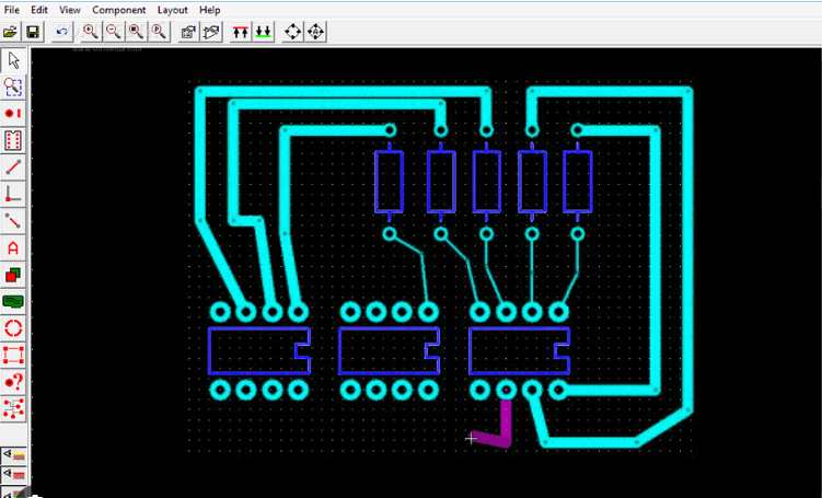
1.4 Routing Techniques
Routing involves connecting components based on the schematic netlist. Different routing strategies include:
- Manual Routing: Provides full control over trace paths but is time-consuming.
- Auto-Routing: Faster but may require manual optimization for critical signals.
- High-Speed Routing: Requires controlled impedance, length matching, and differential pair routing.
1.4.1 Power and Ground Routing
- Power Planes: Use solid planes for stable power distribution.
- Ground Planes: Essential for noise reduction and signal integrity.
- Decoupling Capacitors: Place near IC power pins to suppress noise.
1.4.2 Signal Integrity Considerations
- Impedance Control: Match trace width and dielectric properties for high-speed signals.
- Differential Pairs: Route with consistent spacing to maintain signal balance.
- Avoiding Crosstalk: Increase spacing between parallel traces or use ground shielding.
1.5 Design Rule Check (DRC) and Verification
Before finalizing the PCB layout, perform:
- Electrical Rule Check (ERC): Ensures no open or short circuits.
- Design Rule Check (DRC): Validates trace width, spacing, and manufacturing constraints.
- Signal Integrity Analysis: Simulates high-speed signal behavior.
2. Key Points in PCB Layout Design
2.1 Signal Integrity and EMI Mitigation
- Proper Grounding: Use a low-impedance ground plane to reduce noise.
- Shielding: Enclose sensitive signals with ground traces or vias.
- Minimizing Loop Areas: Reduce electromagnetic interference (EMI) by keeping return paths short.
2.2 Thermal Management
- Thermal Vias: Help dissipate heat from high-power components.
- Copper Pours: Increase heat dissipation in power sections.
- Component Spacing: Avoid clustering heat-sensitive parts near hot components.
2.3 Manufacturing and Assembly Considerations
- Design for Manufacturability (DFM): Follow PCB fabrication guidelines (e.g., minimum trace width, hole sizes).
- Solder Mask and Silkscreen: Ensure clear markings for assembly and debugging.
- Test Points: Include accessible test points for validation and troubleshooting.
2.4 High-Speed Design Techniques
- Controlled Impedance Routing: Critical for RF and high-speed digital signals.
- Length Matching: Ensures synchronous signal arrival (e.g., DDR memory).
- Via Optimization: Minimize via stubs to reduce signal reflections.
2.5 Power Distribution Network (PDN) Design
- Low-Impedance Power Delivery: Use multiple vias and wide traces for power paths.
- Decoupling Strategy: Place capacitors at different frequency ranges for noise suppression.
3. Advanced PCB Layout Techniques
3.1 Multilayer PCB Design
- Layer Stackup Planning: Assign signal, power, and ground layers strategically.
- Microstrip and Stripline Routing: Used for impedance-controlled traces in high-speed designs.
3.2 Flexible and Rigid-Flex PCBs
- Bend Radius Considerations: Ensure traces can withstand mechanical stress.
- Stiffener Placement: Reinforces areas where components are mounted.
3.3 HDI (High-Density Interconnect) PCBs
- Blind and Buried Vias: Increase routing density in compact designs.
- Laser Drilling: Enables finer pitch components and tighter routing.
4. Conclusion
PCB layout design is a complex but essential process that impacts the performance, reliability, and manufacturability of electronic devices. By following systematic design methods—such as proper schematic capture, strategic component placement, controlled routing, and thorough verification—engineers can achieve optimal PCB designs. Additionally, considering signal integrity, thermal management, and manufacturing constraints ensures a robust and high-quality PCB.
As technology advances, PCB designers must stay updated with emerging trends such as HDI, flexible PCBs, and advanced high-speed design techniques to meet the demands of modern electronics


