PCB Layout for Switching Regulator Design
Switch-mode power supplies are used to convert one voltage to another. The efficiency of this type of power supply is usually very high, so in many applications, it replaces linear regulators.
Switching Frequency and Switching Transitions
Switching-mode power supplies operate at a certain switching frequency. The switching frequency can be fixed (such as in PWM type control) or can vary according to certain factors (such as in PFM or hysteresis type control). In either case, the working principle of a switch-mode power supply is that it has a certain on time Ton and a certain off time Toff. A typical switching cycle with a 50% duty cycle. This means that for 50% of the complete cycle T, there is a certain current in the converter; for the other 50% of the time, there is a different current in the converter.
The actual switching frequency (in other words, the cycle length T) is not very important when we consider system noise. If it is within the sensitive signal frequency range of the system, the switching frequency or its harmonics may affect the system. But in general, the switching frequency is not the biggest factor affecting the system.
In a switch-mode power supply, what really matters is the speed of the switching transitions. We can see a zoomed-in picture of the switching transitions on a time scale. On a time scale with a period T of 2us, for a 500kHz PWM switching frequency, the transition looks like a vertical line. But when zoomed in, we can see that the switching transitions typically take 30 to 90ns.

Why is good PCB layout important?
Every 2.5cm of PCB trace has a trace inductance of about 20nH. The exact inductance value depends on the thickness, width, and geometry of the trace, but as a rule of thumb, 20nH/2.5cm is generally practical. Assuming a buck regulator provides 5A output current, we will see the current switch from 0A to 5A. When the switching current is large and the switching transition time is short, we can use the following formula to calculate how much voltage offset the tiny trace inductance will produce:
Assuming the trace is 2.5cm long (20nH), the output current is 5A (5A switching current in the buck regulator), and the transition time of the MOSFET power switch is 30ns, the voltage offset will be 3.33V.
As can be seen, only 2.5cm of trace inductance can produce a considerable voltage offset. This offset often even causes the switch mode power supply to fail completely. Placing the input capacitor a few centimeters away from the input pins of the switch regulator will often cause the switch mode power supply to not work. On a board with improper layout and routing, if the switch mode power supply still works, it will generate very large electromagnetic interference (EMI).
In the above formula, the only parameter we can change is the trace inductance. We can reduce the trace inductance by making the trace as short as possible. Thicker copper wire also helps to reduce inductance. Since the power required by the load is fixed, we cannot change the current parameters. We can change the transition time, but we generally don’t want to. Slowing down the transition time reduces the voltage offset generated, thus reducing EMI, but the switching losses will increase and we will have to operate at a lower switching frequency and with expensive and bulky power devices.

Finding the AC Current Routes
The most important rule in the PCB layout of a switch mode power supply is to keep the AC traces as short as possible in some way. If this rule is followed carefully, a good board layout can be said to be 80% successful. In order to find these AC traces that change the current from “full current” to “no current” in a very short time (transition time), we draw the schematic three times. It is a simple step-down switch mode power supply. In the top schematic, we draw the current flow during the on time with a dotted line. In the middle schematic, we draw the current flow during the off time with a dotted line. The bottom schematic is particularly noteworthy. Here, we draw all the traces where the current changes from the on time to the off time.
In this way, we can easily find the AC current traces for any switch mode power supply topology.
When evaluating an existing board layout, a good idea is to print it out on paper, place a clear plastic sheet over it, and then use different colored pens to draw the current flow and corresponding AC traces for the on and off times. While we tend to think we can do this relatively simple task in our heads, we often make small mistakes in our thinking process, so it is highly recommended to draw the traces on paper.
Achieving Good PCB Layout
AC traces for buck regulators. It is important to note that some ground traces are also AC traces and need to be kept as short as possible. In addition, it is recommended not to use any vias for these AC current paths, as the inductance of vias is also quite high. There are very few exceptions to this rule. If not using vias for the AC path will actually result in a higher trace inductance than the via itself, then it is recommended to use vias. Multiple vias in parallel are better than using only a single via.
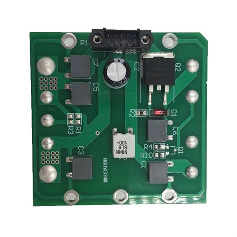
Layout example of a board using the Analog Devices ADP2300 buck regulator. Let’s check that the AC traces in the diagram are routed along the absolute shortest possible paths.
Connection A is routed along the shortest possible path because the high-side connection of C2 can be connected to the switching MOSFET (pin 5 of the ADP2300, the Vin pin) with the shortest possible trace.
Connection B is the trace between pin 6 (SW pin) and the cathode side of diode D1. Again, we see that this trace is as short as possible to reduce trace inductance.
Connection C is the trace between the anode of diode D1 and the ground connection of C2. The pads of these two devices are adjacent to each other, which has the lowest trace inductance. It is also beneficial for this AC current not to flow through the quiet ground plane. The ground plane should only be used as a reference voltage, and it is best if no current (especially no AC current) flows through the ground plane. The vias next to C2 connect the ground area on the top layer of the PCB to the ground on the bottom layer, but no AC current flows through these vias.
Special Considerations for Inductors
We must also consider inductors when it comes to EMI. Actual devices are not as symmetrical as many people believe. An inductor has a core with wire wrapped around it. The winding always has a start and an end. The start is connected to the inner winding of the inductor and the end is connected to the outer winding of the inductor. Figure 4 shows a typical drum inductor schematic. The start of the winding is usually marked with a dot on the device. It is important to connect the start to the noisy switch node and the end to a quiet voltage. For a buck regulator, the quiet voltage is the output voltage. This way, the fixed voltage on the outer winding can electrically shield the AC switch node voltage on the inner winding, so the EMI of the power supply will be low.
By the way, the same is true for so-called shielded inductors. Shielded inductors with a certain magnetic permeability do use some kind of shielding material on the outside, which tightens most of the magnetic field lines on the package side. However, this material can only suppress magnetic fields, not electric fields. AC voltage on the outer winding is mainly a problem caused by electrical or capacitive coupling, and the shielding material of the shielded inductor does not suppress such coupling. Therefore, the shielded inductor should also be placed on the board so that the noisy switch node is connected to the start of the winding to minimize EMI.
The Basics of Good PCB Layout for Switch-Mode Power Supplies
Engineering courses do not generally teach how to achieve good PCB layout. High-frequency RF courses will study the importance of trace impedance, but engineers who need to build their own system power supplies do not usually think of power supplies as high-frequency systems and ignore the importance of PCB layout. Most problems caused by improper PCB layout can be attributed to not keeping the AC current traces as short and compact as possible. Understanding the reasoning behind the PCB layout guidelines described in this article and strictly following them will minimize any PCB-related problems with switch-mode power supplies.