Pcb layout software
Top Features To Look For In PCB Layout Software
When selecting PCB layout software, it is crucial to consider a range of features that can significantly impact the efficiency and quality of your design process.
One of the primary features to look for is an intuitive user interface.
A well-designed interface can streamline the workflow, making it easier for both novice and experienced designers to navigate the software. This ease of use can reduce the learning curve and allow for quicker adaptation to the tool, ultimately saving time and resources.
Another essential feature is the software’s ability to handle complex designs.
As electronic devices become more sophisticated, the need for advanced design capabilities grows. Therefore, the software should support multi-layer PCB designs, high-density interconnects, and various component types. This flexibility ensures that the software can accommodate a wide range of projects, from simple circuits to intricate systems.
Integration with other design tools is also a critical factor.
PCB layout software should seamlessly integrate with schematic capture tools, simulation software, and mechanical CAD programs. This interoperability allows for a more cohesive design process, enabling designers to move effortlessly between different stages of development. Additionally, it facilitates better collaboration among team members who may be using different tools.
Design rule checking (DRC) is another indispensable feature.
DRC helps ensure that the PCB layout adheres to specific manufacturing and performance standards. By automatically checking for errors such as spacing violations, trace width issues, and other design constraints, DRC can prevent costly mistakes and rework. This feature not only enhances the reliability of the final product but also accelerates the design process by catching errors early.
Moreover, the ability to perform real-time design analysis is highly beneficial.
Features such as signal integrity analysis, thermal analysis, and power integrity analysis can provide immediate feedback on the performance of the PCB design. This real-time analysis helps identify potential issues before they become problematic, allowing for timely adjustments and optimizations.
Component libraries are another vital aspect to consider.
A comprehensive and up-to-date component library can significantly expedite the design process. The software should offer a vast selection of components, complete with accurate footprints and electrical characteristics. Furthermore, the ability to import custom components or update libraries from manufacturers ensures that designers have access to the latest parts and technologies.
Collaboration features are increasingly important in today’s interconnected world.
PCB layout software should support version control, multi-user access, and cloud-based storage. These features enable teams to work together more effectively, regardless of their physical location. Version control ensures that changes are tracked and managed, reducing the risk of errors and miscommunication.
Lastly, consider the software’s support and documentation.
Comprehensive documentation, tutorials, and customer support can be invaluable resources, especially when encountering complex design challenges. Access to a robust support network can make a significant difference in the overall user experience, providing assistance when needed and ensuring that designers can make the most of the software’s capabilities.
In conclusion, selecting the right PCB layout software involves evaluating a range of features that contribute to an efficient and effective design process. An intuitive user interface, advanced design capabilities, integration with other tools, design rule checking, real-time analysis, comprehensive component libraries, collaboration features, and robust support are all critical factors to consider. By carefully assessing these features, designers can choose software that meets their specific needs and enhances their ability to create high-quality PCB designs.
Comparing Popular PCB Layout Software: Pros And Cons
Printed Circuit Board (PCB) layout software is an essential tool for electronics engineers and designers, enabling them to create intricate and functional circuit designs. As the demand for more sophisticated electronic devices grows, so does the need for advanced PCB layout software. Several popular options are available, each with its own set of advantages and disadvantages. Understanding these can help professionals make informed decisions about which software best suits their needs.
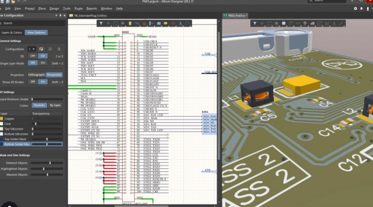
One of the most widely used PCB layout software is Altium Designer.
Known for its comprehensive suite of tools, Altium Designer offers a robust platform for both schematic capture and PCB layout. Its user-friendly interface and extensive library of components make it a favorite among many engineers. Additionally, Altium Designer supports 3D visualization, which allows designers to view their boards in a three-dimensional space, facilitating better design accuracy and error detection. However, the software’s high cost can be a significant drawback, particularly for small businesses or individual users. Moreover, its extensive features can be overwhelming for beginners, requiring a steep learning curve.
In contrast, Eagle PCB, developed by Autodesk, is another popular choice, especially among hobbyists and small-scale designers.
Eagle PCB is known for its affordability and flexibility, offering a free version with limited features and a more comprehensive paid version. The software’s modular design allows users to add or remove features as needed, making it highly customizable. Furthermore, Eagle PCB’s integration with Autodesk’s Fusion 360 provides seamless transition between electronic and mechanical design. Despite these advantages, Eagle PCB has some limitations, such as a less intuitive user interface compared to Altium Designer and fewer advanced features, which may not meet the needs of more complex projects.
KiCad is an open-source PCB layout software that has gained popularity due to its cost-effectiveness and community-driven development.
Being open-source, KiCad is free to use, making it an attractive option for students, hobbyists, and small businesses. The software offers a comprehensive set of tools for schematic capture, PCB layout, and even 3D visualization. Additionally, KiCad’s active user community contributes to continuous improvements and updates. However, the open-source nature of KiCad means that official support is limited, relying instead on community forums and user-generated documentation. This can be a disadvantage for users who require immediate assistance or professional support.
Another notable mention is OrCAD, developed by Cadence Design Systems.
OrCAD is renowned for its powerful simulation capabilities and extensive component libraries. It is particularly favored in industries where precision and reliability are paramount, such as aerospace and automotive sectors. OrCAD’s advanced features, such as signal integrity analysis and thermal simulation, provide designers with the tools needed to create highly reliable and efficient PCBs. On the downside, OrCAD’s complexity and high cost can be prohibitive for smaller projects or less experienced users. The software’s steep learning curve also means that significant time investment is required to become proficient.
In summary, the choice of PCB layout software depends largely on the specific needs and constraints of the user. Altium Designer offers a comprehensive and feature-rich platform but comes with a high price tag. Eagle PCB provides a more affordable and flexible option, though it may lack some advanced features. KiCad stands out as a cost-effective, open-source solution with a strong community backing, while OrCAD excels in precision and reliability for high-stakes industries. By carefully weighing the pros and cons of each software, designers can select the most appropriate tool to bring their electronic projects to life.
How To Optimize Your PCB Layout For Better Performance
Optimizing your PCB layout for better performance is a critical aspect of electronic design that can significantly impact the functionality, reliability, and efficiency of your final product. To achieve an optimal layout, it is essential to consider several key factors, including component placement, signal integrity, power distribution, and thermal management. By addressing these elements systematically, you can enhance the overall performance of your printed circuit board (PCB).
Firstly, component placement is a fundamental step in PCB layout optimization.
Proper placement of components can minimize signal path lengths, reduce electromagnetic interference (EMI), and improve thermal dissipation. It is advisable to place high-speed components close to each other to minimize signal delay and potential interference. Additionally, grouping components with similar functions can simplify routing and reduce the complexity of the layout. For instance, placing decoupling capacitors near their respective integrated circuits (ICs) can help stabilize voltage levels and filter out noise.
Transitioning to signal integrity, it is crucial to ensure that signals are transmitted without degradation.
This can be achieved by maintaining controlled impedance for high-speed signal traces and avoiding sharp bends that can cause signal reflections. Utilizing differential pairs for high-speed signals can also enhance signal integrity by reducing noise and crosstalk. Furthermore, maintaining adequate spacing between signal traces can prevent unwanted coupling and interference. Employing ground planes and proper grounding techniques can further improve signal integrity by providing a low-impedance return path for signals.
Power distribution is another critical aspect of PCB layout optimization.
Ensuring that power is delivered efficiently to all components requires careful planning of power and ground planes. Using wide traces or planes for power distribution can reduce voltage drops and minimize resistance. Additionally, placing vias strategically can help distribute power evenly across different layers of the PCB. It is also important to consider the placement of power supply components, such as voltage regulators and decoupling capacitors, to ensure stable and clean power delivery.
Thermal management is an often-overlooked but vital component of PCB layout optimization.
Effective thermal management can prevent overheating and ensure the longevity and reliability of electronic components. To achieve this, it is essential to consider the thermal properties of the materials used in the PCB and the placement of heat-generating components. Utilizing thermal vias, heat sinks, and copper pours can help dissipate heat more effectively. Additionally, arranging components to allow for adequate airflow can further enhance thermal management.
In addition to these key factors, it is beneficial to use advanced PCB layout software tools that offer features such as design rule checks (DRC), signal integrity analysis, and thermal simulation.
These tools can help identify potential issues early in the design process and provide insights into how to optimize the layout for better performance. By leveraging these software tools, designers can make informed decisions and implement best practices more effectively.
In conclusion, optimizing your PCB layout for better performance involves a comprehensive approach that addresses component placement, signal integrity, power distribution, and thermal management. By carefully considering these factors and utilizing advanced PCB layout software tools, designers can create high-performance, reliable, and efficient PCBs. This systematic approach not only enhances the functionality of the final product but also contributes to its overall success in the market.
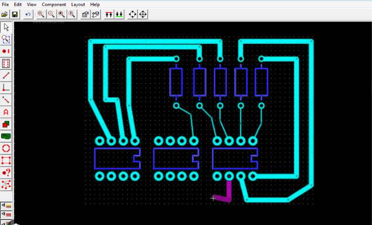
Beginner’s Guide To Using PCB Layout Software
Printed Circuit Board (PCB) layout software is an essential tool for anyone involved in electronics design, from hobbyists to professional engineers. Understanding how to use this software effectively can significantly enhance the efficiency and accuracy of your design process. This guide aims to provide beginners with a comprehensive overview of the fundamental aspects of PCB layout software, ensuring a smooth transition into the world of electronic design automation.
To begin with, it is crucial to recognize that PCB layout software serves as a bridge between the conceptual design of an electronic circuit and its physical realization.
The software allows users to create detailed schematics, place components, and route electrical connections on a virtual board. This digital representation is then used to manufacture the actual PCB. Therefore, mastering the basics of PCB layout software is a vital step in bringing your electronic projects to life.
One of the first steps in using PCB layout software is to familiarize yourself with its interface.
Most PCB design tools, such as Eagle, KiCad, and Altium Designer, offer a user-friendly interface that includes a schematic editor and a layout editor. The schematic editor is where you will draw the circuit diagram, while the layout editor is used to design the physical PCB. It is advisable to spend some time exploring these editors, as understanding their functionalities will make the design process more intuitive.
Once you are comfortable with the interface, the next step is to create a new project and start designing your schematic.
This involves selecting and placing components from the software’s library onto the schematic editor. Components such as resistors, capacitors, and integrated circuits are represented by symbols, which you can connect using wires to form the desired circuit. It is important to ensure that all connections are correctly made, as errors at this stage can lead to issues in the final PCB.
After completing the schematic, the next phase is to transfer it to the layout editor.
This process, often referred to as “netlist generation,” involves converting the schematic into a format that the layout editor can understand. In the layout editor, you will place the physical footprints of the components onto the PCB and route the electrical connections between them. This step requires careful consideration of factors such as component placement, trace width, and signal integrity to ensure optimal performance of the final product.
Throughout the design process, it is essential to perform regular checks and validations.
Most PCB layout software includes tools for design rule checking (DRC) and electrical rule checking (ERC), which help identify potential issues such as short circuits, unconnected pins, and violations of spacing rules. Utilizing these tools can save you time and effort by catching errors early in the design process.
Finally, once you are satisfied with your design, the last step is to generate the necessary files for manufacturing.
These files, commonly known as Gerber files, contain all the information required to produce the PCB, including the layout, drill holes, and solder mask. It is crucial to review these files carefully before sending them to a manufacturer to ensure that they accurately represent your design.
In conclusion, using PCB layout software effectively involves understanding its interface, creating accurate schematics, transferring designs to the layout editor, performing regular checks, and generating manufacturing files. By following these steps, beginners can confidently navigate the complexities of PCB design and bring their electronic projects to fruition.


