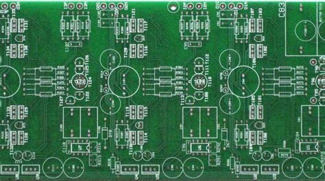
PCB Layout Style Mistakes That can Ruin Your design
Modern pcb layout software allows engineers,designers,and hobbyists to quickly and easily design pcbs.This software provides creative freedom,but sometime this isn’t good thing.PCB designers can make careless design mistakes that don’t affect the product’s functionality but can hinder assembly,debugging,and yield because these mistakes create confusion.This article explains some basic careless pcb design style mistakes and how to avoid them.
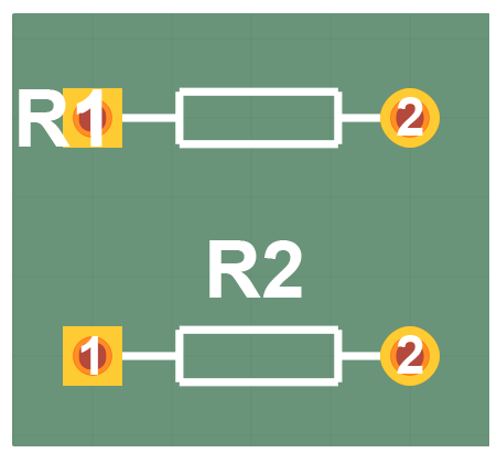
Reference Markers under Pads
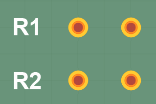
Reference designators placed on copper will appear in the PCB layout software but not on the physical PCB.If your reference designators are placed over pads in the layout ,they will be lost when you get the PCB,making component placement difficult.In the image below,the reference designer for R1 is not printed completely on the PCB.The”1″ is clipped off.The reference designator forR2 is correctly placed.
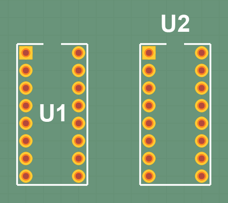
Reference Marker under the package
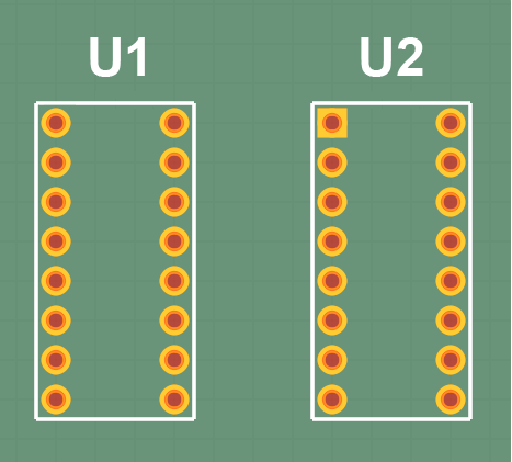
If you place reference marks under a component,you or your contract manufacturer may be able to place the component,but if you need to remove or replace a component for repair or debugging,it will be difficult to find the component on the pcb. In the image below,after U1 is placed on the PCB.In the image below,after U1 is placed on the pcb,U1’s reference mark in hidden.After U2 is placed,U2’s reference mark is clearly is clearly visible.
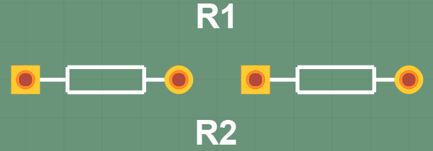
Reference Markers Not Clearly Assigned to Components
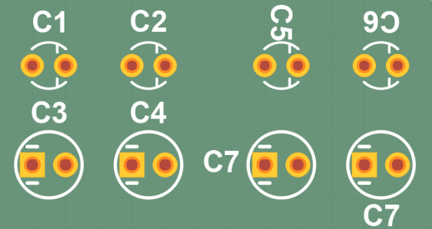
Placed reference marks as close to their components as possible.Place reference designators in a way that makes it clear which components they belong to.Failure to do so will make it difficult to place the correct component in the correct location.This is important for assembly and debugging.In the image below,it is unclear which resistor is R1 and which is R2.
Reference Designators with small fonts
Use a reference designator font that is large enough to be easily read.The author has successfully used a font that is least 0.060”tall and 0.050”wide.This tip does not include a picture,as reference designators of any size look good on large ,high-resolution displays,especially when zoomed in.
Components Close to Each Other with Ambiguous Reference Designators
Placing componet next to each other without reference deisgnators clearly indicating which component goes on which pad can lead to a number of problems,including the wrong components being placed in an unintended manner,introducing shorts or opens.The author has seen layout with this error,as shown in the image below.Some pcb made using this layout assembled correctly with horizontally placed resistors.Other PCBs had resistors placed incorrectly vertically.This component misalignment caused the PCB to not function.Using package with outlines around the components is one way to avoid this problem.
Reference Markers with Random Orientations
Reference markers on a PCB should face one or more directions. Randomly oriented reference designators make assembly and debugging more difficult because components are harder to find. The component on the left has a properly placed reference designator. The component on the right has a reference designator with a different orientation, which is a bad idea.
Pin 1 is not marked on the integrated circuit
Integrated circuits should have a clear indicator, such as a dot or star, next to pin 1 to ensure the IC is installed correctly. Improperly installed ICs can be damaged or destroyed. When the IC is on the PCB, debugging is easier if the pin 1 indicator is not buried underneath the IC. In the image below, U1 will be difficult to place correctly. Notice that the pin numbers you see in the image do not appear on the PCB. U2 will be placed correctly because pin 1 is clearly marked (square pin).
Not Marking the Polarity of Polarized Components
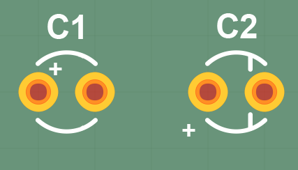
Some two-terminal components, such as LEDs and electrolytic capacitors, are polarized. Improperly installing polarized components can cause circuit malfunction or component damage. LEDs only illuminate when installed correctly. If installed upside down, the LED will not conduct and may even be damaged by voltage breakdown. Electrolytic capacitors can explode if reverse biased. Use footprints to indicate polarity. Polarity markings should not be buried under components. In the image below, the footprint of C1 is poor because the polarity marking is covered by the component. The footprint of C2 is good because the polarity marking is visible when the capacitor is on the PCB.
Placing components too close together
Placing components too close together can lead to problems such as solder bridges. If components are too close together, probing with an oscilloscope or multimeter can be difficult because the probes may short multiple components together. Placing components too close together can also make replacing components difficult. This can be seen on PCBs, where component spacing may appear fine on large displays.
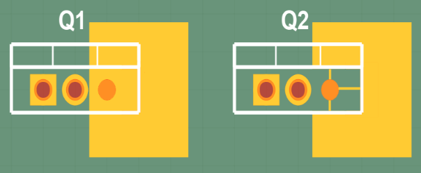
Not Using Heatsinks
Using heatsinks on component pins makes soldering easier. You might not want to use heatsinks to reduce electrical resistance and thermal impedance, but not using them can make soldering very difficult, especially when component pads are connected to large traces or copper fill. Without proper heatsinking, large traces and copper fill act as heat sinks, making heating the pad difficult. In the image below, Q1’s source pin has no heatsink. This MOSFET can be difficult to solder and desolder. Q2’s source pin has a heatsink. This MOSFET is easy to solder and desolder. PCB designers can change the amount of heatsinking to control the electrical resistance and thermal impedance of the connection. For example,
Understand the limitations of your PCB manufacturer, contract manufacturer, and you
Have a good set of design rules that your PCB manufacturer can meet.
Find out if you or your CM can handle difficult packages like ball grid arrays. If you’re doing the soldering yourself, packages with legs extending out to the side of the IC package are easier to solder, especially if the pitch isn’t too small (less than 0.100″).
Conclusion
This article covered some PCB layout style issues that can cause assembly and debugging problems. Remember to carefully place reference marks, use a good package with polarity and pin 1 markings, use heat sinks, and consider manufacturing constraints when designing. Following these good design practices will make assembly easier, improve yield, and make debugging easier. These benefits can save time, money, and give you peace of mind.