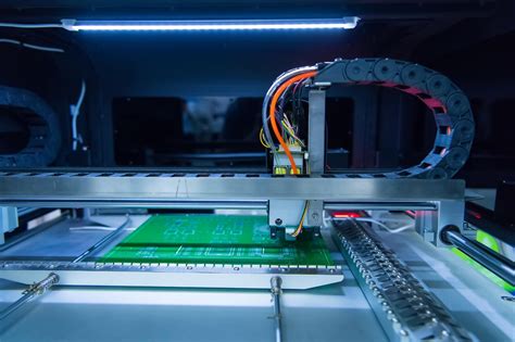
Pcb making with 3D printer
Essential Tools And Materials For DIY PCB Manufacturing
Creating printed circuit boards (PCBs) at home has become increasingly accessible due to advancements in technology and the availability of essential tools and materials. For enthusiasts and professionals alike, understanding the necessary components and equipment is crucial for successful DIY PCB manufacturing. This article will explore the fundamental tools and materials required for this intricate process, ensuring a comprehensive understanding for those embarking on this endeavor.
To begin with, the foundation of any PCB project is the design software.
Programs such as Eagle, KiCad, and Altium Designer are popular choices, offering robust features for schematic capture and PCB layout. These tools allow users to create detailed designs, which can then be exported as Gerber files, the industry standard for PCB manufacturing. Transitioning from design to physical creation, the next step involves transferring the design onto a copper-clad board.
Copper-clad boards, typically made of fiberglass or phenolic resin, are essential for PCB manufacturing.
These boards are coated with a thin layer of copper, which will form the conductive pathways of the circuit. To transfer the design onto the board, a laser printer and glossy paper are often used. The design is printed onto the glossy paper using toner, which is then transferred to the copper-clad board through a process called toner transfer. This method requires a laminator or a household iron to apply heat and pressure, ensuring the toner adheres to the copper surface.
Once the design is transferred, the next critical step is etching.
Etching removes the unwanted copper, leaving only the desired circuit pathways. Ferric chloride is a commonly used etchant, although alternatives like ammonium persulfate or cupric chloride are also effective. Safety precautions are paramount during this stage, as these chemicals can be hazardous. Proper ventilation, gloves, and eye protection are essential to ensure safe handling.
After etching, the board must be cleaned to remove any residual toner and etchant.
Acetone or isopropyl alcohol can be used for this purpose, revealing the clean copper traces. Drilling is the subsequent step, where holes for component leads and vias are created. A precision drill press or a Dremel tool with appropriate drill bits is necessary for this task. Accurate drilling is crucial for component placement and soldering.
Soldering is the final step in assembling the PCB. A high-quality soldering iron with adjustable temperature control is indispensable. Solder wire, flux, and a soldering stand are also required. Flux helps to clean the surfaces and improve the flow of solder, ensuring strong electrical connections. Additionally, a desoldering pump or braid can be useful for correcting mistakes.
In conclusion, DIY PCB manufacturing demands a range of specialized tools and materials, each playing a vital role in the process. From design software and copper-clad boards to etching chemicals and soldering equipment, each component must be carefully selected and utilized. By understanding and acquiring these essential tools and materials, hobbyists and professionals can successfully create custom PCBs at home, fostering innovation and creativity in electronics projects.
Step-By-Step Guide To Designing Your Own PCB
Designing your own printed circuit board (PCB) at home can be a rewarding and educational experience, allowing you to bring your electronic projects to life with a high degree of customization. The process, while intricate, can be broken down into manageable steps that ensure a successful outcome. To begin with, it is essential to have a clear understanding of the circuit you wish to create. This involves drafting a schematic diagram, which serves as a blueprint for your PCB. Software tools such as Eagle, KiCad, or Altium Designer are invaluable at this stage, providing a platform to design and simulate your circuit before moving on to the physical creation.
Once your schematic is complete, the next step is to convert it into a PCB layout.
This involves placing the components on a virtual board and routing the electrical connections between them. It is crucial to consider factors such as component placement, trace width, and the overall size of the board. Proper component placement can significantly impact the performance and reliability of your PCB, so it is advisable to follow best practices, such as keeping high-frequency components close together and minimizing the length of critical signal paths.
After finalizing the layout, the next phase is to generate the Gerber files, which are the standard format for PCB manufacturing.
These files contain all the necessary information about the board’s layers, including the copper traces, solder mask, and silkscreen. Most PCB design software can export Gerber files directly, ensuring that they are ready for the manufacturing process.
With the Gerber files in hand, you can now move on to the actual fabrication of the PCB.
For home-based manufacturing, there are several methods available, each with its own set of advantages and challenges. One popular method is the toner transfer process, which involves printing the PCB layout onto a special transfer paper using a laser printer. The printed layout is then transferred onto a copper-clad board using heat, typically from an iron or a laminator. After the transfer, the board is etched in a chemical solution, such as ferric chloride, to remove the unwanted copper, leaving behind the desired circuit traces.
Another method is the photoresist technique, which offers higher precision and is suitable for more complex designs.
This process involves coating the copper-clad board with a photosensitive material and then exposing it to ultraviolet light through a transparent film of the PCB layout. The exposed areas harden, while the unexposed areas remain soluble and can be washed away, leaving the desired pattern. The board is then etched in a similar manner to the toner transfer process.
Once the etching is complete, the next step is to drill holes for through-hole components and vias.
A precision drill press or a handheld rotary tool can be used for this purpose. After drilling, the board should be thoroughly cleaned to remove any residual chemicals and debris.
The final stage involves soldering the components onto the board.
This requires a steady hand and a good-quality soldering iron. It is important to follow the schematic carefully to ensure that each component is placed correctly and that all connections are secure. After soldering, it is advisable to inspect the board for any solder bridges or cold joints that could affect the performance of the circuit.
In conclusion, designing and manufacturing your own PCB at home is a detailed process that requires careful planning and execution. By following these steps and utilizing the appropriate tools and techniques, you can create a functional and reliable PCB tailored to your specific needs.
Common Mistakes To Avoid In Home PCB Fabrication
When embarking on the journey of home PCB fabrication, it is essential to be aware of common mistakes that can compromise the quality and functionality of your printed circuit boards.
One prevalent error is the improper handling of materials.
Ensuring that you use high-quality copper-clad boards and appropriate etching chemicals is crucial. Low-grade materials can lead to poor conductivity and unreliable connections, which can ultimately result in circuit failure. Additionally, it is important to store these materials in a controlled environment to prevent oxidation and contamination.
Another frequent mistake is neglecting the importance of accurate design and layout.
Utilizing PCB design software can significantly enhance precision, but it is vital to double-check your design for errors before proceeding to fabrication. Overlooking design rules, such as trace width and spacing, can lead to short circuits or signal integrity issues. Furthermore, failing to incorporate proper grounding techniques can result in electromagnetic interference, which can degrade the performance of your circuit.
Transitioning to the fabrication process, one must be cautious about the etching stage. I
nadequate etching can leave behind unwanted copper, causing shorts and connectivity problems. Conversely, over-etching can erode necessary traces, leading to open circuits. It is essential to monitor the etching process closely and use a timer to ensure consistency. Additionally, agitating the etching solution can help achieve a more uniform etch, reducing the likelihood of defects.
Drilling holes for component leads is another critical step where precision is paramount.
Using a drill press or a high-speed rotary tool can provide better control compared to a handheld drill. Misaligned or improperly sized holes can make component placement difficult and affect the overall integrity of the solder joints. It is advisable to use a drill bit size that matches the component leads to ensure a snug fit.
Soldering is an area where many beginners encounter difficulties.
Cold solder joints, caused by insufficient heat or poor technique, can lead to unreliable connections. It is important to use a temperature-controlled soldering iron and to apply the right amount of solder. Excessive solder can create bridges between adjacent pads, while too little solder can result in weak joints. Practicing good soldering techniques, such as heating the pad and the component lead simultaneously, can help achieve strong and reliable connections.
Another common oversight is inadequate testing and inspection.
Before powering up your PCB, it is crucial to perform a thorough visual inspection to identify any obvious defects, such as solder bridges or missing components. Using a multimeter to check for continuity and proper voltage levels can help identify potential issues before they cause damage to your components. Additionally, testing your circuit in stages can make troubleshooting easier and more efficient.
Finally, it is important to consider the environmental impact of your home PCB fabrication process.
Proper disposal of chemicals and waste materials is essential to minimize harm to the environment. Following local regulations and guidelines for hazardous waste disposal can help ensure that your hobby does not have a negative impact on the planet.
In conclusion, by being mindful of these common mistakes and taking proactive steps to avoid them, you can improve the quality and reliability of your home-fabricated PCBs. Attention to detail, proper technique, and thorough testing are key components of successful PCB fabrication. With practice and diligence, you can achieve professional-level results in your home workshop.
Cost-Effective Methods For Etching PCBs At Home
Creating printed circuit boards (PCBs) at home can be a cost-effective and rewarding endeavor for electronics enthusiasts and hobbyists. The process of etching PCBs, which involves transferring a circuit design onto a copper-clad board and then removing unwanted copper, can be accomplished using several methods. Each method has its own set of advantages and challenges, and understanding these can help you choose the most suitable approach for your needs.
One of the most popular methods for etching PCBs at home is the toner transfer method.
This technique involves printing the circuit design onto a special toner transfer paper using a laser printer. The printed design is then transferred onto the copper-clad board by applying heat, typically with a household iron or a laminator. The heat causes the toner to adhere to the copper surface, creating a resist that protects the copper underneath during the etching process.
After the transfer, the board is submerged in an etching solution, commonly ferric chloride or a mixture of hydrochloric acid and hydrogen peroxide, which dissolves the exposed copper, leaving behind the desired circuit pattern. This method is favored for its simplicity and relatively low cost, although it requires careful handling of chemicals and precise control of the heat application.
Another effective method for etching PCBs at home is the photoresist method.
This approach uses a photosensitive material to create the resist pattern on the copper-clad board. The process begins by coating the board with a layer of photoresist, which can be either a liquid or a dry film. The circuit design, printed on a transparent sheet, is then placed over the coated board and exposed to ultraviolet (UV) light. The UV light hardens the photoresist in the areas corresponding to the circuit design, while the unexposed areas remain soft and can be washed away with a developer solution. The board is then etched in a similar manner to the toner transfer method. The photoresist method is known for its high precision and ability to produce fine details, making it suitable for more complex circuit designs. However, it requires additional equipment such as a UV light source and can be more time-consuming.
For those seeking an even more straightforward approach, the direct inkjet printing method offers a viable alternative.
This technique involves using an inkjet printer modified to print directly onto the copper-clad board with etch-resistant ink. The printed design acts as the resist during the etching process. This method eliminates the need for transfer papers or photoresist materials, simplifying the workflow. However, it requires a specialized printer and ink, which can be an initial investment. Additionally, achieving consistent results may require some experimentation and fine-tuning of the printer settings.
In conclusion, etching PCBs at home can be achieved through various cost-effective methods, each with its own set of benefits and considerations. The toner transfer method is accessible and straightforward, making it ideal for beginners. The photoresist method offers high precision and is suitable for intricate designs, albeit with a more involved process. The direct inkjet printing method simplifies the workflow but requires specialized equipment. By understanding these methods and their respective requirements, you can select the most appropriate technique for your PCB projects, enabling you to create custom circuit boards efficiently and economically.


