PCB Manual Layout Considerations: Best Practices and Key Points
Introduction
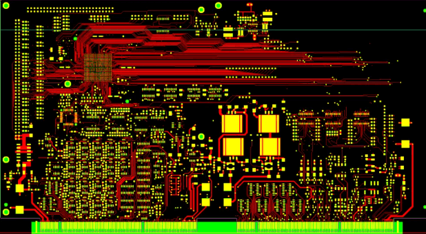
Printed Circuit Board (PCB) layout is a critical step in electronic design, determining the performance, reliability, and manufacturability of the final product. While automated tools like autorouters can assist in PCB design, manual layout remains essential for high-speed, high-frequency, and complex designs. A well-executed manual layout ensures signal integrity, reduces electromagnetic interference (EMI), and improves thermal management.
This article explores key considerations for PCB manual layout, including component placement, routing strategies, grounding techniques, and design for manufacturability (DFM).
1. Component Placement
Proper component placement is the foundation of an efficient PCB layout. Poor placement can lead to signal integrity issues, increased noise, and thermal problems.
1.1. Functional Grouping
- Group related components (e.g., power supply, analog, digital, RF) to minimize trace lengths and reduce interference.
- Place high-speed components (e.g., processors, memory) close to their supporting circuitry (e.g., decoupling capacitors, clock sources).
1.2. Thermal Considerations
- Position heat-generating components (e.g., voltage regulators, power transistors) near the board edge or with adequate airflow.
- Use thermal vias under hot components to dissipate heat efficiently.
1.3. Mechanical Constraints
- Ensure components fit within enclosure dimensions.
- Avoid placing tall components near board edges where they may interfere with mounting.
1.4. Signal Flow Optimization
- Arrange components to follow a logical signal path, minimizing crossovers and long traces.
- Keep high-frequency traces short to reduce parasitic inductance and capacitance.
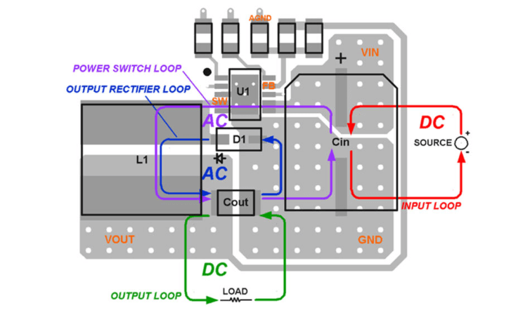
2. Power and Grounding Strategies
A robust power distribution network (PDN) is crucial for stable operation.
2.1. Power Plane Design
- Use dedicated power planes for different voltage levels (e.g., 3.3V, 5V, 12V).
- Avoid splitting power planes unnecessarily, as this can increase impedance.
2.2. Grounding Techniques
- Implement a solid ground plane to minimize ground loops and noise.
- Use star grounding for mixed-signal designs to separate analog and digital grounds.
- Avoid ground cuts under high-speed signals to prevent impedance discontinuities.
2.3. Decoupling Capacitors
- Place decoupling capacitors as close as possible to IC power pins.
- Use multiple capacitors (e.g., 0.1µF, 1µF, 10µF) to filter different noise frequencies.
3. Signal Routing and Trace Design
Proper trace routing ensures signal integrity and reduces EMI.
3.1. Trace Width and Current Capacity
- Calculate trace width based on current requirements (use IPC-2152 standards).
- Wider traces reduce resistance and heat buildup in high-current paths.
3.2. Impedance Control
- Match trace impedance for high-speed signals (e.g., USB, HDMI, DDR).
- Use controlled dielectric materials and proper trace spacing for differential pairs.
3.3. Avoiding Crosstalk
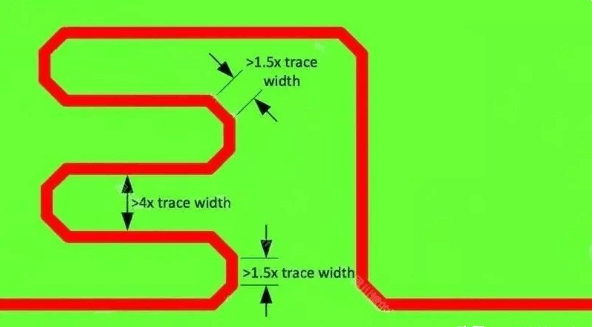
- Maintain adequate spacing between parallel traces (3x trace width is a common rule).
- Route sensitive signals (e.g., clock lines) away from noisy traces (e.g., switching power supplies).
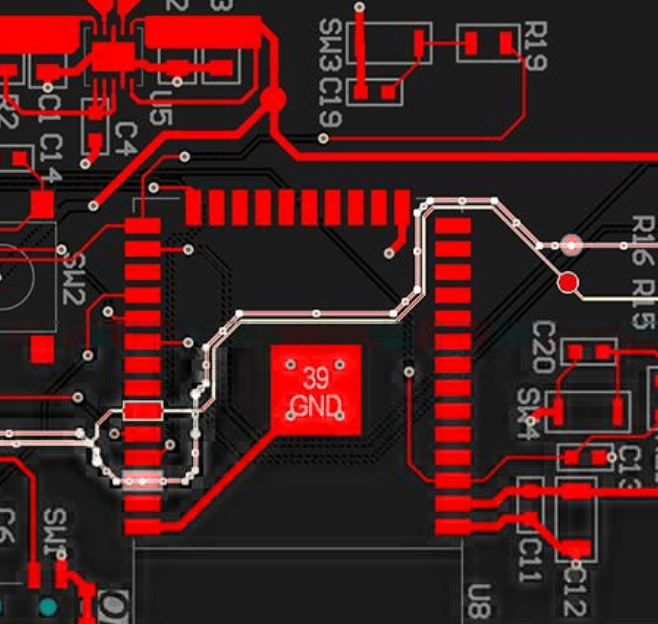
3.4. Minimizing Vias
- Excessive vias increase inductance and signal reflections.
- Use fewer vias in high-speed paths and avoid placing them in differential pairs.
3.5. Right-Angle Traces
- Avoid 90° angles in high-frequency traces; use 45° bends instead to reduce impedance discontinuities.
4. EMI and Noise Reduction
Electromagnetic interference (EMI) can degrade performance and cause compliance failures.
4.1. Shielding and Grounding
- Use ground planes to shield sensitive traces.
- Enclose high-frequency circuits with grounded copper pours.
4.2. Loop Area Minimization
- Keep high-current return paths short to reduce loop inductance.
- Route differential pairs closely together to cancel magnetic fields.
4.3. Filtering and Ferrite Beads
- Add ferrite beads or LC filters to suppress high-frequency noise in power lines.
- Use bypass capacitors near ICs to filter high-frequency noise.
5. Design for Manufacturability (DFM)
A well-designed PCB should be easy to manufacture and assemble.
5.1. Component Spacing
- Follow manufacturer guidelines for minimum spacing between components.
- Ensure enough clearance for soldering and rework.
5.2. Solder Mask and Silkscreen
- Apply solder mask to prevent accidental shorts.
- Use clear silkscreen markings for component orientation and test points.
5.3. Panelization Considerations
- Include fiducial marks for automated assembly.
- Add breakaway tabs or mouse bites for depaneling.
5.4. Test Points and Debugging
- Provide accessible test points for critical signals.
- Label test points for easier debugging.
6. High-Speed Design Considerations
For high-frequency PCBs (e.g., RF, DDR, PCIe), additional precautions are necessary.
6.1. Controlled Impedance Routing
- Use microstrip or stripline configurations for impedance matching.
- Simulate trace impedance before fabrication.
6.2. Length Matching
- Match trace lengths for differential pairs and high-speed buses to prevent skew.
6.3. Via Stitching
- Use via stitching in ground planes to reduce return path discontinuities.
Conclusion
Manual PCB layout requires careful planning to ensure optimal performance, manufacturability, and reliability. By following best practices in component placement, power distribution, signal routing, and EMI reduction, designers can create high-quality PCBs that meet both electrical and mechanical requirements.
While automated tools can assist, a well-executed manual layout remains essential for complex and high-performance designs. By considering these key factors, engineers can minimize design iterations and produce robust PCBs for a wide range of applications.
Would you like any specific section expanded further?