Pcb manufacturing capabilities
Advanced Techniques In PCB Manufacturing
Printed Circuit Board (PCB) manufacturing has evolved significantly over the years, driven by the increasing complexity and miniaturization of electronic devices. Advanced techniques in PCB manufacturing have become essential to meet the stringent demands of modern electronics, ensuring high performance, reliability, and efficiency.
One of the most notable advancements in this field is the development of High-Density Interconnect (HDI) technology.
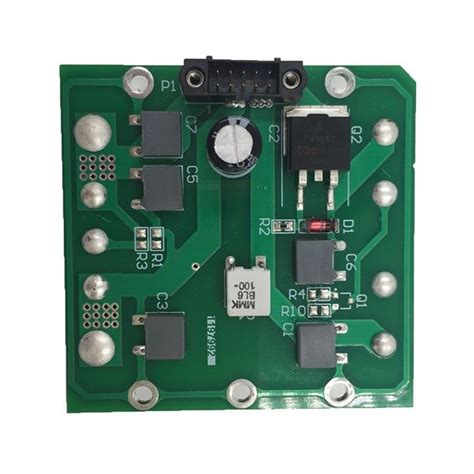
HDI PCBs utilize finer lines and spaces, smaller vias, and higher connection pad density, allowing for more components to be placed on a smaller board. This technology is particularly beneficial for applications where space is at a premium, such as in smartphones, tablets, and other compact electronic devices.
Another critical advancement is the use of flexible and rigid-flex PCBs.
These boards combine the benefits of both rigid and flexible substrates, providing enhanced design versatility and improved mechanical performance. Flexible PCBs can be bent and folded to fit into unconventional spaces, making them ideal for wearable technology, medical devices, and aerospace applications. Rigid-flex PCBs, on the other hand, offer the structural integrity of rigid boards while maintaining the flexibility needed for dynamic applications. This combination reduces the need for connectors and cables, thereby improving signal integrity and reducing overall system weight.
The implementation of advanced materials has also played a significant role in enhancing PCB manufacturing capabilities.
High-frequency laminates, for instance, are designed to support high-speed signal transmission with minimal loss, making them suitable for high-frequency applications such as radar systems, satellite communications, and 5G technology. Additionally, the use of advanced thermal management materials helps dissipate heat more effectively, ensuring the longevity and reliability of electronic components in high-power applications.
Laser drilling technology has revolutionized the process of creating microvias, which are essential for HDI PCBs.
Traditional mechanical drilling methods are not suitable for the fine features required in modern PCBs. Laser drilling, however, offers precision and accuracy, enabling the creation of microvias with diameters as small as 50 micrometers. This technique not only improves the electrical performance of the PCB but also allows for more complex and compact designs.
Surface finish technologies have also seen significant advancements, with options such as Electroless Nickel Immersion Gold (ENIG), Immersion Silver, and Organic Solderability Preservative (OSP) becoming more prevalent.
These finishes provide excellent solderability, corrosion resistance, and surface planarity, which are crucial for reliable component assembly and long-term performance. The choice of surface finish depends on the specific requirements of the application, including factors such as cost, environmental considerations, and compatibility with lead-free soldering processes.
Moreover, the advent of advanced inspection and testing techniques has greatly improved the quality and reliability of PCBs.
Automated Optical Inspection (AOI) and Automated X-ray Inspection (AXI) systems are now commonly used to detect defects such as open circuits, short circuits, and misaligned components. These systems provide high-resolution imaging and real-time analysis, ensuring that any issues are identified and rectified early in the manufacturing process. Additionally, electrical testing methods such as Flying Probe Testing and In-Circuit Testing (ICT) are employed to verify the electrical functionality of the PCB, further enhancing its reliability.
In conclusion, the advancements in PCB manufacturing techniques have significantly expanded the capabilities of modern electronics. From HDI technology and flexible PCBs to advanced materials and precision drilling, these innovations have enabled the production of smaller, more powerful, and more reliable electronic devices. As technology continues to evolve, it is expected that PCB manufacturing will continue to advance, meeting the ever-growing demands of the electronics industry.
Innovations In High-Density Interconnect (HDI) PCBs
High-Density Interconnect (HDI) printed circuit boards (PCBs) represent a significant advancement in the field of electronics manufacturing, offering enhanced performance and miniaturization capabilities. As the demand for more compact and efficient electronic devices continues to grow, HDI PCBs have emerged as a critical solution, enabling the integration of more components in a smaller footprint. This innovation is driven by several key manufacturing capabilities that distinguish HDI PCBs from traditional PCBs.
One of the primary features of HDI PCBs is the use of microvias, which are significantly smaller than conventional vias.
Microvias allow for higher wiring density and improved electrical performance by reducing the distance that signals must travel. This reduction in signal path length minimizes signal loss and enhances the overall speed and reliability of the electronic device. Furthermore, the ability to place microvias directly on component pads, known as via-in-pad technology, contributes to the efficient use of space and further miniaturization of the PCB.
In addition to microvias, HDI PCBs often incorporate multiple layers of interconnections, which are achieved through advanced lamination techniques.
These multilayer structures enable the stacking of several layers of circuitry, allowing for more complex designs and greater functionality within a limited area. The use of sequential lamination processes, where additional layers are added one at a time, ensures precise alignment and connectivity between layers, which is crucial for maintaining the integrity of high-density circuits.
Another critical aspect of HDI PCB manufacturing is the use of advanced materials that support high-frequency and high-speed applications.
These materials, such as low-loss dielectrics and high-performance substrates, are essential for maintaining signal integrity and reducing electromagnetic interference (EMI). The selection of appropriate materials is a key consideration in the design and fabrication of HDI PCBs, as it directly impacts the performance and reliability of the final product.
Moreover, the precision required in HDI PCB manufacturing necessitates the use of state-of-the-art equipment and techniques.
Laser drilling, for instance, is commonly employed to create microvias with high accuracy and consistency. This method allows for the production of extremely small and precise holes, which are essential for the high-density interconnects characteristic of HDI PCBs. Additionally, advanced imaging and inspection technologies, such as automated optical inspection (AOI) and X-ray inspection, are utilized to ensure the quality and reliability of the intricate circuitry.
The benefits of HDI PCBs extend beyond their physical and electrical properties.
The ability to integrate more functionality into a smaller space translates to cost savings in terms of materials and assembly. Furthermore, the enhanced performance and reliability of HDI PCBs contribute to the overall longevity and efficiency of electronic devices, making them an attractive option for a wide range of applications, from consumer electronics to aerospace and medical devices.
In conclusion, the innovations in HDI PCB manufacturing capabilities have revolutionized the electronics industry, enabling the development of smaller, faster, and more reliable devices. The use of microvias, multilayer interconnections, advanced materials, and precision manufacturing techniques are key factors that contribute to the superior performance of HDI PCBs. As technology continues to evolve, the demand for high-density interconnect solutions is expected to grow, driving further advancements in PCB manufacturing and paving the way for the next generation of electronic devices.
The Role Of Automation In PCB Production
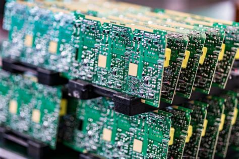
The role of automation in PCB production has become increasingly significant as the demand for high-quality, reliable, and cost-effective printed circuit boards (PCBs) continues to grow. Automation in PCB manufacturing encompasses a wide range of processes, from design and prototyping to assembly and testing, each contributing to the overall efficiency and precision of the production cycle. By integrating advanced technologies and automated systems, manufacturers can achieve greater consistency, reduce human error, and enhance productivity, ultimately leading to superior end products.
One of the primary benefits of automation in PCB production is the improvement in design accuracy and efficiency.
Computer-aided design (CAD) software allows engineers to create detailed and precise PCB layouts, which can then be directly translated into manufacturing instructions. This eliminates the need for manual drafting and significantly reduces the likelihood of design errors. Furthermore, automated design tools can perform complex calculations and simulations, ensuring that the final product meets all necessary specifications and performance criteria.
Transitioning from design to prototyping, automation continues to play a crucial role.
Rapid prototyping technologies, such as 3D printing and automated milling machines, enable manufacturers to quickly produce and test PCB prototypes. This accelerates the development process and allows for iterative testing and refinement, ensuring that any issues are identified and resolved early in the production cycle. As a result, manufacturers can bring new products to market more swiftly and with greater confidence in their performance and reliability.
In the assembly phase, automation is indispensable for achieving high levels of precision and consistency.
Automated pick-and-place machines are capable of accurately positioning and soldering components onto the PCB at high speeds, far surpassing the capabilities of manual assembly. These machines are equipped with advanced vision systems that can detect and correct misalignments, ensuring that each component is placed correctly. Additionally, automated soldering techniques, such as reflow and wave soldering, provide consistent and reliable connections, further enhancing the quality of the final product.
Testing and inspection are critical stages in PCB production, and automation has revolutionized these processes as well.
Automated optical inspection (AOI) systems use high-resolution cameras and sophisticated algorithms to examine PCBs for defects, such as solder bridges, missing components, and misalignments. These systems can quickly and accurately identify issues that might be overlooked during manual inspection, ensuring that only fully functional boards proceed to the next stage of production. Moreover, automated testing equipment can perform electrical tests to verify the functionality of the PCB, providing an additional layer of quality assurance.
The integration of automation in PCB production also offers significant cost benefits.
By reducing the reliance on manual labor, manufacturers can lower production costs and minimize the risk of human error. Automated systems can operate continuously, increasing throughput and enabling manufacturers to meet tight deadlines and high-volume demands. Additionally, the enhanced precision and consistency achieved through automation result in fewer defects and rework, further reducing costs and improving overall efficiency.
In conclusion, the role of automation in PCB production is multifaceted and transformative. From design and prototyping to assembly and testing, automated systems enhance accuracy, efficiency, and reliability at every stage of the manufacturing process. As technology continues to advance, the capabilities of automated PCB production will only expand, enabling manufacturers to meet the ever-growing demands of the electronics industry with greater precision and cost-effectiveness. The continued adoption of automation in PCB manufacturing is not only a testament to its benefits but also a necessary evolution to keep pace with the rapid advancements in electronic technology.
Quality Control Measures In PCB Fabrication
In the realm of printed circuit board (PCB) fabrication, quality control measures are paramount to ensuring the reliability and performance of the final product. The intricate nature of PCBs, which serve as the backbone of virtually all electronic devices, necessitates rigorous quality control protocols throughout the manufacturing process. These measures are designed to detect and mitigate potential defects, thereby enhancing the overall integrity and functionality of the PCBs.
To begin with, the initial stage of PCB fabrication involves the careful selection of raw materials.
High-quality substrates, copper foils, and laminates are essential to the production of robust PCBs. Suppliers are meticulously vetted, and materials are subjected to stringent incoming inspection procedures. This preliminary step is crucial, as the use of substandard materials can lead to significant issues down the line, such as delamination or poor electrical performance.
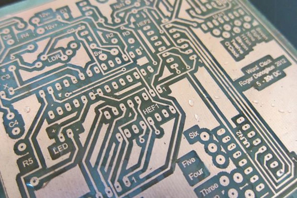
Following the procurement of materials, the PCB manufacturing process advances to the design and layout phase.
Here, design for manufacturability (DFM) guidelines are employed to ensure that the PCB design is optimized for production. DFM considerations include trace width, spacing, and the placement of components, all of which are critical to preventing manufacturing defects. Advanced software tools are utilized to simulate and validate the design, thereby identifying potential issues before the physical fabrication begins.
As the process transitions to the actual fabrication of the PCB, several quality control measures are implemented to monitor each step.
During the etching process, for instance, automated optical inspection (AOI) systems are employed to detect any discrepancies in the copper traces. AOI systems use high-resolution cameras and sophisticated algorithms to compare the etched patterns against the original design files, ensuring that any deviations are promptly identified and rectified.
Subsequently, the PCBs undergo a series of electrical tests to verify their functionality.
One of the most common methods is the flying probe test, which involves the use of probes to test the electrical continuity and isolation of the PCB traces. This non-destructive testing method is highly effective in identifying open circuits, short circuits, and other electrical faults. Additionally, in-circuit testing (ICT) may be conducted to assess the performance of individual components and their connections.
Thermal stress testing is another critical quality control measure in PCB fabrication.
PCBs are subjected to thermal cycling, which involves repeatedly heating and cooling the boards to simulate real-world operating conditions. This testing helps to identify potential issues related to thermal expansion and contraction, such as solder joint failures or component detachment. By exposing the PCBs to extreme temperatures, manufacturers can ensure that the boards will perform reliably under various environmental conditions.
Moreover, X-ray inspection is employed to examine the internal structures of the PCBs, particularly in multilayer boards where visual inspection is not feasible.
X-ray imaging allows for the detection of hidden defects, such as voids in solder joints or misaligned vias. This non-destructive testing method provides a comprehensive view of the PCB’s internal features, ensuring that any anomalies are addressed before the boards are shipped to customers.
In conclusion, quality control measures in PCB fabrication are integral to producing reliable and high-performance circuit boards. From the selection of raw materials to the final inspection, each step of the manufacturing process is meticulously monitored and controlled. By employing advanced testing methods and adhering to stringent quality standards, PCB manufacturers can deliver products that meet the rigorous demands of modern electronic applications.