PCB Manufacturing-Ceramic PCB-Printed circuit board Process
We are pleased to inform you about our ceramic PCB manufacturing process. Our company
has been providing high-quality ceramic PCBs to various industries for many years.
We take pride in our advanced technology and expertise in producing ceramic PCBs that meet
our customers’ requirements.
Our ceramic PCB manufacturing process involves several stages, each of which is crucial in
ensuring the final product’s quality and reliability. We follow strict quality control measures to
ensure that every ceramic PCB we produce meets our customers’ expectations.

The first stage of our ceramic PCB manufacturing process is the design phase. We work closely
with our customers to understand their requirements and specifications.
Our team of engineers uses advanced software to design the ceramic PCB according to the
customer’s specifications. We ensure that the design meets the required electrical and mechanical
properties.
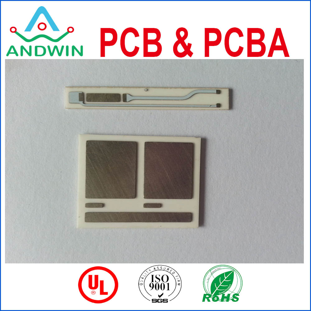
Once the design is finalized, we move on to the next stage, which is the production of the ceramic
substrate. We use high-quality ceramic materials to manufacture the substrate.
The substrate is then cut to the required size and shape using advanced cutting tools.
We ensure that the substrate’s surface is smooth and free from any defects that may affect the final product’s performance.

The next stage is the deposition of the conductive material on the substrate. We use various
methods to deposit the conductive material, such as screen printing, inkjet printing, or laser
direct imaging. We ensure that the conductive material is evenly distributed and has the
required thickness to meet the customer’s specifications.
After the conductive material is deposited, we move on to the etching stage. We use
advanced etching techniques to remove the excess conductive material from the substrate.
We ensure that the etching process does not affect the substrate’s surface or the conductive material’s integrity.

The next stage is the drilling of the holes. We use advanced drilling machines to drill
the required holes in the substrate.
We ensure that the holes are of the required size and are placed in the correct locations.
Once the holes are drilled, we move on to the plating stage. We use various plating techniques to
plate the conductive material on the holes’ walls.
We ensure that the plating thickness is uniform and meets the customer’s specifications.
The final stage is the testing and inspection stage. We test every ceramic PCB we
produce to ensure that it meets the required electrical and mechanical properties.
We also inspect the ceramic PCB for any defects or abnormalities that may affect its performance.
In conclusion, our ceramic PCB manufacturing process involves several stages, each of which is
crucial in ensuring the final product’s quality and reliability.
We take pride in our advanced technology and expertise in producing ceramic PCBs
that meet our customers’ requirements. If you have any questions or would like
to place an order, please do not hesitate to contact us.