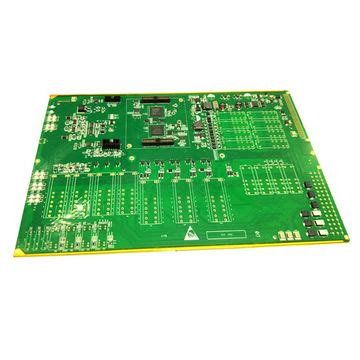
Pcb manufacturing issues
Common Defects in PCB Manufacturing and How to Avoid Them
Printed Circuit Boards (PCBs) are the backbone of modern electronic devices, serving as the foundation upon which electronic components are mounted and interconnected. However, the manufacturing process of PCBs is fraught with potential defects that can compromise the functionality and reliability of the final product. Understanding these common defects and implementing strategies to avoid them is crucial for manufacturers aiming to produce high-quality PCBs.
One prevalent issue in PCB manufacturing is the occurrence of open circuits.
Open circuits arise when there is a break in the conductive path, preventing electrical current from flowing as intended. This defect often results from incomplete etching during the manufacturing process, where the copper layer is not fully removed, leaving unintended gaps. To mitigate this issue, manufacturers should ensure precise control over the etching process, employing advanced techniques such as laser etching to achieve greater accuracy.
In addition to open circuits, short circuits pose a significant challenge.
Short circuits occur when two conductive paths unintentionally connect, allowing current to flow along an unintended route. This defect can lead to overheating and potential damage to the PCB and its components. Short circuits often result from excessive soldering or misalignment of components. To prevent this, manufacturers should implement stringent quality control measures, including automated optical inspection (AOI) systems, to detect and rectify misalignments before they lead to short circuits.
Another common defect is solder bridging, which occurs when excess solder creates a bridge between two adjacent pads, causing an unintended connection.
This issue is particularly prevalent in PCBs with fine-pitch components, where the spacing between pads is minimal. To avoid solder bridging, manufacturers should optimize their solder paste application process, ensuring that the right amount of solder is applied. Additionally, using solder masks can help prevent solder from spreading to unintended areas.
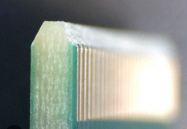
Delamination is another defect that can compromise the structural integrity of a PCB.
This issue arises when layers of the PCB separate, often due to inadequate bonding during the lamination process. Delamination can lead to a loss of electrical connectivity and mechanical strength. To address this, manufacturers should ensure that the lamination process is conducted under optimal conditions, with appropriate pressure and temperature settings. Furthermore, selecting high-quality materials that are compatible with the intended application can reduce the risk of delamination.
Moreover, via failures are a critical concern in PCB manufacturing.
Vias are small holes that allow electrical connections between different layers of a PCB. Failures in vias can occur due to poor plating, leading to incomplete or weak connections. To prevent via failures, manufacturers should employ advanced plating techniques, such as electroplating, to ensure robust and reliable connections. Regular testing and inspection of vias during the manufacturing process can also help identify potential issues early on.
In conclusion, while PCB manufacturing is a complex process with numerous potential defects, understanding these common issues and implementing effective strategies can significantly enhance the quality and reliability of the final product. By focusing on precise etching, stringent quality control, optimized soldering processes, robust lamination, and reliable via connections, manufacturers can minimize defects and produce PCBs that meet the high standards required in today’s electronic devices. As technology continues to advance, staying abreast of the latest manufacturing techniques and materials will be essential for overcoming these challenges and ensuring the continued success of PCB manufacturing.

The Impact of Material Selection on PCB Reliability
In the realm of printed circuit board (PCB) manufacturing, the selection of materials plays a pivotal role in determining the reliability and performance of the final product. As electronic devices become increasingly complex and miniaturized, the demand for PCBs that can withstand various environmental and operational stresses has intensified. Consequently, understanding the impact of material selection on PCB reliability is crucial for manufacturers aiming to produce high-quality, durable products.
To begin with, the choice of substrate material is fundamental to the overall reliability of a PCB.
The substrate serves as the foundation upon which the entire circuit is built, and its properties significantly influence the board’s thermal and mechanical performance. Common substrate materials include FR-4, a glass-reinforced epoxy laminate, which is favored for its balance of cost, performance, and ease of processing. However, for applications requiring higher thermal stability, such as in automotive or aerospace industries, materials like polyimide or ceramic substrates may be preferred due to their superior heat resistance and dimensional stability.
Moreover, the selection of conductive materials is equally critical.
Copper is the most widely used conductive material in PCBs due to its excellent electrical conductivity and relatively low cost. However, the thickness and quality of the copper layer can affect the board’s ability to handle current loads and dissipate heat. Thicker copper layers can enhance current-carrying capacity and improve thermal management, but they also increase the board’s weight and cost. Therefore, manufacturers must carefully balance these factors to optimize performance without compromising reliability.
In addition to substrate and conductive materials, the choice of solder mask and surface finish can also impact PCB reliability.
The solder mask, typically a polymer layer applied over the copper traces, protects against oxidation and prevents solder bridges during assembly. The material and thickness of the solder mask can influence the board’s thermal cycling performance and resistance to environmental factors such as moisture and chemicals. Similarly, the surface finish, which provides a protective coating over exposed copper areas, must be selected based on the intended application. Options such as HASL (Hot Air Solder Leveling), ENIG (Electroless Nickel Immersion Gold), and OSP (Organic Solderability Preservative) each offer distinct advantages and limitations in terms of solderability, shelf life, and environmental resistance.
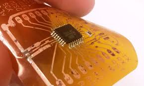
Furthermore, the integration of advanced materials, such as high-frequency laminates and flexible substrates, is becoming increasingly prevalent in modern PCB designs.
These materials enable the development of PCBs for specialized applications, such as high-speed data transmission and wearable electronics. However, their unique properties necessitate careful consideration during the design and manufacturing processes to ensure compatibility with existing production techniques and to maintain reliability under operational conditions.
In conclusion, the impact of material selection on PCB reliability cannot be overstated. As the electronics industry continues to evolve, manufacturers must remain vigilant in their choice of materials to meet the growing demands for performance and durability. By understanding the interplay between different materials and their influence on PCB characteristics, manufacturers can make informed decisions that enhance the reliability and longevity of their products. This, in turn, not only satisfies customer expectations but also contributes to the advancement of technology in various sectors.
Troubleshooting Signal Integrity Problems in PCBs
In the realm of printed circuit board (PCB) manufacturing, signal integrity issues present a significant challenge that can compromise the performance and reliability of electronic devices. Signal integrity refers to the quality and reliability of electrical signals as they travel through the PCB. When these signals are distorted or degraded, it can lead to malfunctions, data errors, and even complete system failures. Therefore, understanding and troubleshooting signal integrity problems is crucial for ensuring the optimal performance of PCBs.
One of the primary causes of signal integrity issues is impedance mismatch.
Impedance is the resistance a circuit offers to the flow of alternating current, and when there is a mismatch between the source, transmission line, and load, it can result in signal reflections. These reflections can cause interference and signal degradation, leading to data loss or corruption. To address this, it is essential to ensure that the impedance is matched across all components of the PCB. This can be achieved through careful design and layout, as well as the use of appropriate materials and components.
Another common issue affecting signal integrity is crosstalk, which occurs when a signal in one trace induces an unwanted signal in an adjacent trace.
This can be particularly problematic in high-density PCBs where traces are closely packed. To mitigate crosstalk, designers can increase the spacing between traces, use differential signaling, or implement shielding techniques. Additionally, maintaining a consistent ground plane can help reduce the effects of crosstalk by providing a stable reference point for signals.
Signal attenuation is another factor that can impact signal integrity.
As signals travel through the PCB, they can lose strength due to resistance, dielectric losses, and other factors. This attenuation can be exacerbated by long trace lengths and high-frequency signals. To combat signal attenuation, designers can minimize trace lengths, use low-loss materials, and employ signal amplification techniques where necessary. Furthermore, ensuring that traces are of uniform width and thickness can help maintain signal strength and reduce losses.
Electromagnetic interference (EMI) is also a significant concern in PCB design, as it can disrupt signal integrity by introducing noise into the system.
EMI can originate from both external sources, such as nearby electronic devices, and internal sources, such as switching power supplies. To minimize EMI, designers can use shielding, filtering, and grounding techniques. Additionally, careful component placement and routing can help reduce the susceptibility of the PCB to electromagnetic interference.
Thermal management is another critical aspect of maintaining signal integrity in PCBs.
Excessive heat can cause changes in material properties, leading to variations in impedance and increased signal loss. To address thermal issues, designers can use heat sinks, thermal vias, and other cooling methods to dissipate heat effectively. Moreover, selecting materials with good thermal conductivity can help maintain stable operating conditions and prevent signal degradation.
In conclusion, troubleshooting signal integrity problems in PCBs requires a comprehensive understanding of the various factors that can affect signal quality. By addressing issues such as impedance mismatch, crosstalk, signal attenuation, electromagnetic interference, and thermal management, designers can enhance the performance and reliability of their PCBs. Through careful design, material selection, and implementation of best practices, it is possible to mitigate signal integrity issues and ensure the successful operation of electronic devices.
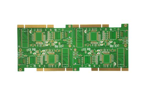
Quality Control Techniques in PCB Production
In the realm of electronics, printed circuit boards (PCBs) serve as the foundational building blocks, facilitating the connection and functionality of various components. As the demand for more sophisticated and reliable electronic devices grows, the importance of quality control in PCB manufacturing becomes increasingly paramount. Ensuring the integrity and performance of PCBs is not merely a matter of meeting industry standards but also a critical factor in maintaining the reputation and competitiveness of manufacturers. Consequently, a comprehensive understanding of quality control techniques is essential for addressing the myriad of challenges that arise during PCB production.
To begin with, one of the primary quality control techniques employed in PCB manufacturing is visual inspection.
This method involves scrutinizing the boards for visible defects such as misalignments, soldering issues, and surface irregularities. While visual inspection is a fundamental step, it is often complemented by automated optical inspection (AOI) systems. AOI systems utilize high-resolution cameras and advanced algorithms to detect defects with greater precision and speed than manual inspection alone. By identifying potential issues early in the production process, manufacturers can mitigate the risk of costly rework or product failures.
In addition to visual inspection, electrical testing plays a crucial role in quality control.
This technique involves verifying the electrical integrity of the PCB by checking for open circuits, short circuits, and other anomalies that could compromise functionality. Flying probe testers and in-circuit testers are commonly used tools in this regard, offering a non-destructive means of ensuring that each board meets the required electrical specifications. By employing these testing methods, manufacturers can ensure that the PCBs will perform reliably in their intended applications.
Moreover, X-ray inspection is another vital quality control technique, particularly for detecting hidden defects in multilayer PCBs.
This non-destructive method allows for the examination of internal structures, such as solder joints and vias, which are not visible through traditional inspection methods. By providing a detailed view of the internal composition of the board, X-ray inspection helps identify potential issues that could lead to failures in the field. This technique is especially valuable in the production of high-density interconnect (HDI) boards, where the complexity of the design necessitates a more thorough examination.
Furthermore, environmental testing is an essential component of quality control in PCB manufacturing.
This involves subjecting the boards to various environmental conditions, such as temperature extremes, humidity, and vibration, to assess their durability and performance under real-world conditions. By simulating these scenarios, manufacturers can identify potential weaknesses and make necessary adjustments to enhance the reliability of the final product. Environmental testing is particularly important for PCBs used in critical applications, such as aerospace and medical devices, where failure is not an option.
In conclusion, quality control techniques in PCB production are multifaceted and require a combination of visual inspection, electrical testing, X-ray inspection, and environmental testing to ensure the highest standards of reliability and performance. By implementing these techniques, manufacturers can address the challenges inherent in PCB production and deliver products that meet the ever-evolving demands of the electronics industry. As technology continues to advance, the importance of rigorous quality control in PCB manufacturing will only grow, underscoring the need for ongoing innovation and improvement in these critical processes.