Pcb manufacturing notes
Best Practices For PCB Design And Layout
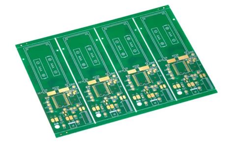
In the realm of electronics, the design and layout of printed circuit boards (PCBs) are critical to the performance and reliability of the final product. To ensure optimal functionality, it is essential to adhere to best practices during the PCB design and layout process.
One of the foremost considerations is the selection of appropriate materials.
The choice of substrate, copper thickness, and solder mask can significantly impact the electrical performance and durability of the PCB. Therefore, it is crucial to select materials that align with the specific requirements of the application.
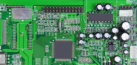
Transitioning to the design phase, component placement is a fundamental aspect that demands meticulous attention.
Proper placement not only facilitates efficient routing but also minimizes potential issues such as signal interference and thermal management challenges. It is advisable to place components with similar functions in close proximity to each other. For instance, analog and digital components should be segregated to prevent noise interference. Additionally, high-frequency components should be positioned to minimize the length of signal paths, thereby reducing potential signal degradation.
Moving forward, the routing of traces is another critical element in PCB design.
The width and spacing of traces must be carefully calculated to handle the required current without causing overheating or signal loss. Utilizing wider traces for power and ground connections can enhance the overall stability of the circuit. Moreover, maintaining consistent trace widths and avoiding sharp angles can prevent issues related to signal integrity. Employing a ground plane is also a best practice that can significantly reduce electromagnetic interference (EMI) and improve signal quality.
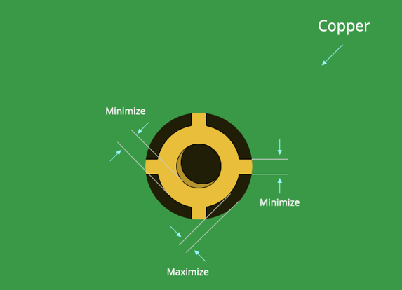
Furthermore, the implementation of vias is an essential consideration in multilayer PCB designs.
Vias facilitate connections between different layers of the PCB, but their placement and size must be optimized to avoid unnecessary complexity and potential signal integrity issues. Blind and buried vias can be employed to save space and improve routing efficiency, but they should be used judiciously due to their higher manufacturing costs.
Thermal management is another critical aspect that cannot be overlooked.
Components that generate significant heat should be strategically placed to ensure adequate heat dissipation. Incorporating thermal vias, heat sinks, and copper pours can aid in managing heat effectively. Additionally, conducting thermal simulations during the design phase can help identify potential hotspots and allow for preemptive design adjustments.
Transitioning to the final stages of the design process, conducting thorough design rule checks (DRCs) is imperative.
DRCs help identify potential issues related to trace widths, spacing, and other design parameters that could lead to manufacturing defects or operational failures. Utilizing advanced PCB design software with robust DRC capabilities can streamline this process and ensure compliance with industry standards.
In conclusion, adhering to best practices in PCB design and layout is paramount to achieving a reliable and high-performance electronic product. From material selection and component placement to trace routing and thermal management, each step plays a crucial role in the overall success of the PCB. By meticulously following these guidelines and leveraging advanced design tools, designers can mitigate potential issues and deliver robust, efficient, and cost-effective PCB solutions.
Common PCB Manufacturing Defects And How To Avoid Them
Printed Circuit Boards (PCBs) are the backbone of modern electronic devices, providing the necessary pathways for electrical currents to flow between various components. However, the manufacturing process of PCBs is intricate and fraught with potential pitfalls. Understanding common PCB manufacturing defects and how to avoid them is crucial for ensuring the reliability and performance of the final product.
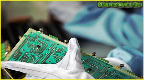
One prevalent defect in PCB manufacturing is solder bridging, which occurs when solder forms an unintended connection between two or more adjacent pads.
This can lead to short circuits and malfunctioning of the electronic device. To mitigate this issue, it is essential to maintain precise control over the soldering process. Utilizing solder masks can help prevent solder from spreading to unintended areas. Additionally, ensuring that the stencil used for solder paste application is accurately aligned and properly maintained can significantly reduce the risk of solder bridging.
Another common defect is the occurrence of open circuits, where there is an unintended break in the electrical pathway.
This can be caused by various factors, including incomplete etching, broken traces, or poor solder joints. To avoid open circuits, it is important to conduct thorough inspections at multiple stages of the manufacturing process. Automated Optical Inspection (AOI) systems can be employed to detect any discontinuities in the traces. Moreover, ensuring that the etching process is carefully controlled and that the PCB design adheres to the manufacturer’s specifications can help prevent open circuits.
Delamination is another issue that can compromise the integrity of a PCB.
This defect involves the separation of the PCB layers, which can be caused by excessive moisture, thermal stress, or poor lamination techniques. To prevent delamination, it is crucial to store PCB materials in a controlled environment with low humidity. Additionally, employing proper lamination techniques and ensuring that the materials used are of high quality can help maintain the structural integrity of the PCB.
Via failures, where the plated through-holes do not form a reliable connection between layers, are also a common defect in PCB manufacturing.
This can result from inadequate plating, contamination, or mechanical stress. To avoid via failures, it is important to ensure that the drilling process is precise and that the holes are properly cleaned before plating. Using high-quality plating materials and techniques can also enhance the reliability of the vias.
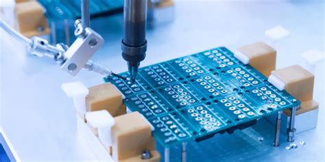
Another significant defect is the misalignment of components, which can lead to poor electrical performance and mechanical instability.
This can be caused by inaccuracies in the placement process or issues with the PCB design. To prevent misalignment, it is essential to use advanced pick-and-place machines that offer high precision. Additionally, designing the PCB with clear and well-defined component footprints can facilitate accurate placement.
Thermal issues, such as overheating or insufficient heat dissipation, can also affect the performance and longevity of a PCB.
These issues can arise from poor thermal management in the design phase or inadequate heat sinking during manufacturing. To address thermal issues, it is important to conduct thermal analysis during the design phase and incorporate appropriate heat dissipation mechanisms, such as thermal vias and heat sinks. Ensuring that the soldering process does not introduce excessive thermal stress can also help maintain the thermal stability of the PCB.
In conclusion, understanding and addressing common PCB manufacturing defects is essential for producing reliable and high-performance electronic devices. By implementing stringent quality control measures, utilizing advanced inspection technologies, and adhering to best practices in PCB design and manufacturing, it is possible to minimize the occurrence of these defects and ensure the success of the final product.
The Importance Of Material Selection In PCB Manufacturing
In the realm of printed circuit board (PCB) manufacturing, the selection of materials plays a pivotal role in determining the performance, reliability, and longevity of the final product. The importance of material selection cannot be overstated, as it directly impacts the electrical, thermal, and mechanical properties of the PCB. Consequently, manufacturers must carefully consider various factors when choosing materials to ensure that the PCB meets the specific requirements of its intended application.
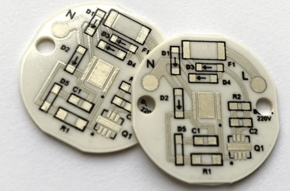
To begin with, the substrate material forms the foundation of the PCB and is crucial for providing structural support and electrical insulation.
The most commonly used substrate material is FR-4, a composite made of woven fiberglass cloth with an epoxy resin binder. FR-4 is favored for its excellent mechanical strength, good electrical insulation properties, and cost-effectiveness. However, for high-frequency applications, materials such as Rogers or Teflon are preferred due to their lower dielectric constant and loss tangent, which minimize signal loss and ensure signal integrity.
Transitioning to the conductive layers, copper is the material of choice for creating the traces and pads that form the electrical connections on the PCB.
Copper’s high electrical conductivity and excellent thermal properties make it ideal for this purpose. The thickness of the copper layer, typically measured in ounces per square foot, is a critical parameter that influences the current-carrying capacity and thermal management of the PCB. For high-power applications, thicker copper layers are necessary to handle the increased current and dissipate heat effectively.
In addition to the substrate and conductive layers, the choice of solder mask material is also significant.
The solder mask is a protective layer applied over the copper traces to prevent short circuits, oxidation, and other environmental damage. Epoxy-based solder masks are widely used due to their durability, chemical resistance, and ease of application. However, for PCBs that require high precision and fine-pitch components, liquid photoimageable (LPI) solder masks are preferred for their superior resolution and ability to create intricate patterns.
Furthermore, the selection of surface finish materials is another critical aspect of PCB manufacturing.
The surface finish protects the exposed copper pads and ensures reliable soldering during component assembly. Common surface finishes include Hot Air Solder Leveling (HASL), Electroless Nickel Immersion Gold (ENIG), and Organic Solderability Preservative (OSP). Each surface finish has its advantages and limitations; for instance, HASL is cost-effective and provides good solderability, but it may not be suitable for fine-pitch components due to its uneven surface. On the other hand, ENIG offers a flat surface and excellent corrosion resistance, making it ideal for high-reliability applications, albeit at a higher cost.
Moreover, the thermal management of the PCB is heavily influenced by the choice of materials.
High-power applications generate significant heat, which must be efficiently dissipated to prevent damage to the components and ensure reliable operation. Materials with high thermal conductivity, such as metal-core PCBs or thermally conductive laminates, are employed to enhance heat dissipation. Additionally, thermal vias and heat sinks are often incorporated into the PCB design to further improve thermal management.
In conclusion, the selection of materials in PCB manufacturing is a multifaceted process that requires careful consideration of various factors, including electrical performance, thermal management, mechanical strength, and cost. By meticulously choosing the appropriate materials, manufacturers can ensure that the PCB meets the specific demands of its application, thereby enhancing its performance, reliability, and longevity. As technology continues to advance, the importance of material selection in PCB manufacturing will only grow, underscoring the need for ongoing research and innovation in this critical area.
Innovations In PCB Manufacturing Technology
Printed Circuit Boards (PCBs) are the backbone of modern electronic devices, serving as the foundation upon which all electronic components are mounted. Over the years, PCB manufacturing technology has undergone significant advancements, driven by the need for more efficient, reliable, and compact electronic devices. One of the most notable innovations in this field is the development of High-Density Interconnect (HDI) technology. HDI PCBs are characterized by their higher wiring density per unit area compared to traditional PCBs. This is achieved through the use of finer lines and spaces, smaller vias, and capture pads, as well as higher connection pad density. The result is a more compact and efficient board that can support the increasing complexity of modern electronics.
Another significant advancement in PCB manufacturing is the adoption of flexible PCBs.
Unlike rigid PCBs, flexible PCBs can bend and fold, allowing for more versatile applications. This flexibility is particularly beneficial in industries such as aerospace, medical devices, and consumer electronics, where space constraints and the need for lightweight components are critical. The use of flexible PCBs has also led to the development of rigid-flex PCBs, which combine the benefits of both rigid and flexible boards, offering enhanced reliability and performance.
In addition to HDI and flexible PCBs, the introduction of advanced materials has also played a crucial role in the evolution of PCB manufacturing.
Traditional PCBs are typically made from materials such as FR4, a composite material composed of woven fiberglass cloth with an epoxy resin binder. However, the demand for higher performance and more durable PCBs has led to the use of advanced materials such as polyimide, Teflon, and ceramic substrates. These materials offer superior thermal stability, electrical performance, and mechanical strength, making them ideal for high-frequency and high-power applications.
The advent of additive manufacturing, commonly known as 3D printing, has also made a significant impact on PCB manufacturing.
3D printing allows for the creation of complex PCB designs that would be difficult or impossible to achieve with traditional manufacturing methods. This technology enables rapid prototyping, reducing the time and cost associated with developing new PCB designs. Furthermore, 3D printing allows for the integration of electronic components directly into the PCB, resulting in more compact and efficient designs.
Another noteworthy innovation is the use of advanced surface finish technologies.
Surface finishes are applied to PCBs to protect the copper circuitry from oxidation and to provide a solderable surface for component attachment. Traditional surface finishes such as Hot Air Solder Leveling (HASL) have been largely replaced by more advanced options such as Electroless Nickel Immersion Gold (ENIG), Immersion Silver, and Organic Solderability Preservative (OSP). These advanced surface finishes offer better performance, reliability, and environmental compliance.
Moreover, the implementation of automated optical inspection (AOI) and automated X-ray inspection (AXI) systems has greatly improved the quality control process in PCB manufacturing.
AOI systems use cameras and image processing software to detect defects in PCBs, while AXI systems use X-rays to inspect the internal structure of PCBs, identifying issues such as voids, misalignments, and solder joint defects. These automated inspection systems ensure that PCBs meet stringent quality standards, reducing the likelihood of failures in the final product.
In conclusion, the continuous advancements in PCB manufacturing technology have significantly enhanced the performance, reliability, and versatility of electronic devices. Innovations such as HDI technology, flexible and rigid-flex PCBs, advanced materials, 3D printing, advanced surface finishes, and automated inspection systems have all contributed to the evolution of PCB manufacturing. As technology continues to advance, it is likely that we will see even more groundbreaking developments in this field, further pushing the boundaries of what is possible in electronic design and manufacturing.