Pcb manufacturing routing
Advanced Techniques In PCB Manufacturing Routing
Printed Circuit Board (PCB) manufacturing has evolved significantly over the years, with routing being one of the most critical aspects of the process. Advanced techniques in PCB manufacturing routing are essential for ensuring optimal performance, reliability, and efficiency of electronic devices. As technology continues to advance, the demand for more complex and compact PCBs has increased, necessitating the adoption of sophisticated routing methods.
One of the primary advanced techniques in PCB routing is the use of high-density interconnect (HDI) technology.
HDI PCBs are characterized by their finer lines and spaces, smaller vias, and higher connection pad density. This technology allows for more components to be placed on a smaller board, which is particularly beneficial for modern electronic devices that require miniaturization without compromising functionality. The implementation of microvias, which are significantly smaller than traditional vias, is a key feature of HDI technology. Microvias enable the creation of more routing layers and improve signal integrity by reducing the length of signal paths.
Another advanced technique is the adoption of differential pair routing.
Differential pairs are pairs of traces that carry equal and opposite signals, which helps to reduce electromagnetic interference (EMI) and crosstalk. This technique is crucial for high-speed digital and analog signals, as it ensures signal integrity and minimizes noise. Properly routing differential pairs involves maintaining consistent trace width, spacing, and length matching, which can be challenging but is essential for achieving optimal performance.
The use of controlled impedance routing is also a significant advancement in PCB manufacturing.
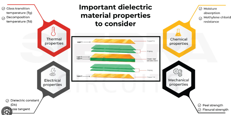
Controlled impedance is the characteristic impedance of a transmission line formed by PCB traces and the surrounding dielectric material. Maintaining controlled impedance is vital for high-frequency signal transmission, as it prevents signal reflections and ensures signal integrity. This technique requires precise control over trace width, spacing, and the dielectric properties of the PCB material. Advanced simulation tools and software are often employed to design and verify controlled impedance traces.
In addition to these techniques, the implementation of via-in-pad technology has become increasingly popular.
Via-in-pad involves placing vias directly within the component pads, which helps to reduce the overall board size and improve thermal and electrical performance. This technique is particularly useful for high-frequency and high-density designs, as it minimizes signal path lengths and reduces inductance. However, via-in-pad requires careful consideration of manufacturing processes, such as via filling and plating, to ensure reliability and prevent solder wicking.
Furthermore, the use of advanced design software and tools has revolutionized PCB routing.
Modern PCB design software offers features such as auto-routing, design rule checks (DRC), and signal integrity analysis, which streamline the routing process and enhance design accuracy. Auto-routing algorithms can quickly generate optimized routing paths based on predefined design rules, saving time and reducing the likelihood of errors. DRC ensures that the design adheres to manufacturing constraints and industry standards, while signal integrity analysis helps identify and mitigate potential issues related to high-speed signal transmission.
In conclusion, advanced techniques in PCB manufacturing routing are essential for meeting the demands of modern electronic devices. The adoption of HDI technology, differential pair routing, controlled impedance routing, via-in-pad technology, and advanced design software has significantly improved the performance, reliability, and efficiency of PCBs. As technology continues to advance, these techniques will play an increasingly important role in the development of innovative and high-performance electronic products.
Common Mistakes To Avoid In PCB Routing
In the intricate process of PCB manufacturing, routing is a critical step that demands precision and expertise. However, even seasoned professionals can fall prey to common mistakes that can compromise the functionality and reliability of the final product.
One prevalent error is the improper management of trace widths.
Ensuring that traces are neither too narrow nor too wide is essential, as this can affect the current-carrying capacity and potentially lead to overheating or signal integrity issues. To mitigate this, designers should adhere to the recommended trace width guidelines based on the current requirements and the type of signals being routed.
Another frequent mistake is the inadequate separation of high-speed and low-speed signals.
Mixing these signals can result in crosstalk, where the electromagnetic interference from high-speed signals disrupts the low-speed signals, leading to data corruption and erratic behavior. To avoid this, it is crucial to maintain sufficient spacing between different signal types and, where possible, use ground planes to shield sensitive traces.
Furthermore, neglecting the importance of return paths can also lead to significant problems.
Every signal trace on a PCB has a corresponding return path, typically through the ground plane. If these return paths are not properly managed, it can cause increased electromagnetic interference (EMI) and signal integrity issues. Designers should ensure that return paths are as short and direct as possible, and avoid creating slots or gaps in the ground plane that could disrupt these paths.
Thermal management is another critical aspect that is often overlooked.
Components that generate significant heat need to be placed strategically to ensure efficient heat dissipation. Failing to do so can result in hotspots that may damage components or affect the overall performance of the PCB. Utilizing thermal vias, heat sinks, and proper component placement can help in managing heat effectively.
Additionally, improper via placement can also pose challenges.
Vias are used to connect different layers of a PCB, but placing them too close to each other or to other components can lead to manufacturing difficulties and potential short circuits. It is advisable to follow the design rules for via placement and ensure that there is adequate clearance around each via.
Another common pitfall is the failure to consider the manufacturability of the PCB design.
Complex designs with tight tolerances can be difficult and expensive to manufacture. Engaging with the PCB manufacturer early in the design process can help identify potential issues and ensure that the design is within the capabilities of the manufacturing process. This collaboration can also help in optimizing the design for cost-effective production.
Lastly, insufficient testing and validation of the PCB design can lead to unforeseen issues during production or in the field.
. Rigorous testing, including signal integrity analysis, thermal analysis, and design rule checks, should be conducted to identify and rectify any potential problems before the design goes into production. This proactive approach can save time and resources by preventing costly rework and ensuring a reliable final product.
In conclusion, avoiding these common mistakes in PCB routing requires a combination of careful planning, adherence to design guidelines, and thorough testing. By paying attention to trace widths, signal separation, return paths, thermal management, via placement, manufacturability, and rigorous testing, designers can enhance the reliability and performance of their PCBs, ultimately leading to successful and efficient electronic products.
The Role Of Software In PCB Routing Optimization
Printed Circuit Board (PCB) manufacturing is a complex process that involves multiple stages, from design to production. One of the most critical aspects of this process is routing, which refers to the layout of electrical connections between various components on the board. The efficiency and effectiveness of PCB routing can significantly impact the performance, reliability, and cost of the final product. In recent years, the role of software in optimizing PCB routing has become increasingly prominent, offering numerous advantages over traditional manual methods.
To begin with, software tools for PCB routing optimization provide designers with advanced algorithms that can handle the intricate task of connecting components while adhering to design rules and constraints.
These algorithms are capable of analyzing multiple routing paths and selecting the most efficient ones, thereby reducing the overall length of the connections and minimizing signal interference. This is particularly important in high-frequency applications where signal integrity is paramount. By leveraging software, designers can achieve a level of precision and accuracy that would be difficult, if not impossible, to attain manually.
Moreover, software for PCB routing optimization often includes features that facilitate the identification and resolution of potential issues early in the design process.
For instance, Design Rule Checking (DRC) is a common feature that automatically verifies whether the routing adheres to predefined rules and standards. This helps in detecting errors such as short circuits, open circuits, and spacing violations before the board goes into production. Consequently, this reduces the likelihood of costly rework and delays, ensuring that the final product meets quality and performance standards.
In addition to error detection, software tools also offer simulation capabilities that allow designers to model and test the electrical behavior of the PCB under various conditions.
This is particularly useful for assessing the impact of routing decisions on parameters such as signal integrity, electromagnetic compatibility, and thermal performance. By simulating different scenarios, designers can make informed decisions and optimize the routing to achieve the desired performance characteristics. This proactive approach not only enhances the reliability of the PCB but also accelerates the design cycle by reducing the need for physical prototypes and iterative testing.
Furthermore, the integration of software in PCB routing optimization streamlines the collaboration between different teams involved in the design and manufacturing process.
Modern software tools often come with features that support version control, real-time collaboration, and seamless data exchange. This ensures that all stakeholders, including electrical engineers, mechanical engineers, and manufacturing personnel, are on the same page and can work together efficiently. The result is a more cohesive and coordinated effort that minimizes errors and accelerates the time-to-market for new products.
Another significant advantage of using software for PCB routing optimization is the ability to handle complex designs with ease.
As electronic devices become more sophisticated and compact, the density of components on PCBs increases, making manual routing increasingly challenging. Software tools can manage these complexities by automating repetitive tasks and providing intelligent suggestions for component placement and routing paths. This not only enhances productivity but also allows designers to focus on more critical aspects of the design, such as functionality and innovation.
In conclusion, the role of software in PCB routing optimization is indispensable in modern PCB manufacturing.
By providing advanced algorithms, error detection, simulation capabilities, and collaborative features, software tools enhance the efficiency, accuracy, and reliability of the routing process. As technology continues to evolve, the integration of software in PCB design and manufacturing will undoubtedly play a crucial role in meeting the growing demands for high-performance and cost-effective electronic products
Innovations In High-Density PCB Routing
In recent years, the field of printed circuit board (PCB) manufacturing has witnessed significant advancements, particularly in the realm of high-density PCB routing. These innovations are driven by the ever-increasing demand for smaller, more powerful electronic devices. As a result, manufacturers are continually seeking new methods to enhance the efficiency and performance of PCBs while maintaining cost-effectiveness and reliability.
One of the most notable innovations in high-density PCB routing is the development of advanced routing algorithms.
These algorithms are designed to optimize the placement and routing of components on a PCB, thereby maximizing the use of available space. By employing sophisticated mathematical models and computational techniques, these algorithms can efficiently navigate the complex web of connections required in high-density designs. This not only reduces the overall size of the PCB but also minimizes signal interference and improves electrical performance.
In addition to advanced routing algorithms, the use of microvias has become increasingly prevalent in high-density PCB designs.
Microvias are small-diameter vias that connect different layers of a PCB, allowing for more compact and efficient routing. Unlike traditional vias, which can take up significant space and potentially introduce signal integrity issues, microvias enable designers to create more intricate and densely packed layouts. This is particularly beneficial in applications where space is at a premium, such as in mobile devices and wearable technology.
Another key innovation in high-density PCB routing is the adoption of high-speed signal integrity techniques.
As electronic devices continue to operate at higher frequencies, maintaining signal integrity becomes increasingly challenging. To address this, manufacturers are implementing techniques such as differential signaling, controlled impedance routing, and the use of advanced materials with low dielectric constants. These methods help to minimize signal loss and crosstalk, ensuring that high-speed signals can travel through the PCB with minimal degradation.
Furthermore, the integration of advanced manufacturing technologies has played a crucial role in the evolution of high-density PCB routing.
Techniques such as laser drilling, precision etching, and additive manufacturing have enabled the production of PCBs with finer features and tighter tolerances. Laser drilling, for instance, allows for the creation of extremely small vias with high precision, which is essential for high-density designs. Precision etching techniques enable the creation of narrow traces and spaces, further enhancing the routing capabilities of modern PCBs. Additive manufacturing, or 3D printing, offers the potential for even greater design flexibility and complexity, opening up new possibilities for high-density PCB routing.
Moreover, the use of advanced simulation and modeling tools has become indispensable in the design and optimization of high-density PCBs.
These tools allow designers to virtually prototype and test their designs before committing to physical production. By simulating the electrical, thermal, and mechanical behavior of a PCB, designers can identify and address potential issues early in the design process. This not only reduces the risk of costly design iterations but also ensures that the final product meets the required performance specifications.
In conclusion, the innovations in high-density PCB routing have significantly transformed the landscape of PCB manufacturing. Advanced routing algorithms, microvias, high-speed signal integrity techniques, and cutting-edge manufacturing technologies have all contributed to the development of more compact, efficient, and reliable PCBs. As the demand for smaller and more powerful electronic devices continues to grow, these innovations will undoubtedly play a critical role in shaping the future of PCB design and manufacturing.