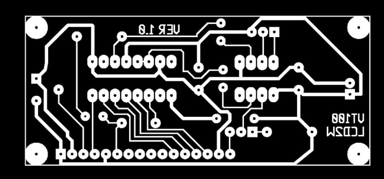
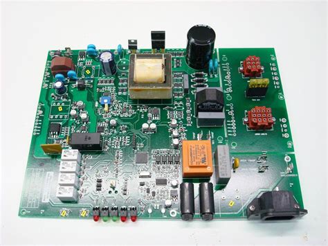
PCB manufacturing routing
Optimizing Trace Widths For Efficient PCB Routing
Optimizing trace widths for efficient PCB routing is a critical aspect of printed circuit board (PCB) design that significantly impacts the performance, reliability, and manufacturability of the final product. The trace width, which refers to the width of the conductive pathways on the PCB, must be carefully calculated to ensure that it can handle the required current without excessive heating or voltage drop. Additionally, the trace width must be compatible with the manufacturing capabilities and constraints of the PCB fabrication process.
To begin with, the current-carrying capacity of a trace is a primary consideration in determining its width.
The trace must be wide enough to carry the maximum expected current without overheating. The IPC-2221 standard provides guidelines for calculating the appropriate trace width based on the current, the allowable temperature rise, and the thickness of the copper layer. For instance, a higher current or a thinner copper layer necessitates a wider trace to prevent excessive heating. Conversely, for lower currents or thicker copper layers, narrower traces may suffice. This balance is crucial to avoid potential failures due to overheating or excessive voltage drops.
Moreover, the electrical performance of the PCB is influenced by the trace width.
Wider traces exhibit lower resistance, which is beneficial for minimizing voltage drops and power losses. However, excessively wide traces can introduce parasitic capacitance and inductance, which may degrade signal integrity, especially in high-frequency applications. Therefore, designers must strike a balance between minimizing resistance and maintaining signal integrity. This often involves using simulation tools to model the electrical behavior of the traces and optimize their widths accordingly.
In addition to electrical considerations, the manufacturability of the PCB imposes constraints on trace widths.
PCB fabrication processes have minimum and maximum trace width limits that must be adhered to. These limits are determined by the capabilities of the etching and plating processes used in manufacturing. For example, very narrow traces may be difficult to etch accurately, leading to potential defects such as breaks or shorts.
On the other hand, very wide traces may require more copper plating, increasing the cost and complexity of the manufacturing process. Therefore, designers must work closely with PCB manufacturers to ensure that the chosen trace widths are within the feasible range for the intended fabrication process.
Furthermore, the layout of the PCB can impact the optimal trace widths.
In densely populated boards, space constraints may necessitate narrower traces to fit all the required connections within the available area. In such cases, designers may need to use multiple layers or employ advanced routing techniques such as microvias to achieve the necessary connectivity without compromising trace width. Conversely, in less densely populated boards, there may be more flexibility to use wider traces, which can simplify the routing process and improve overall reliability.
In conclusion, optimizing trace widths for efficient PCB routing involves a careful balance of electrical, thermal, and manufacturability considerations. Designers must ensure that traces are wide enough to handle the required current without overheating, while also maintaining signal integrity and adhering to manufacturing constraints. By leveraging industry standards, simulation tools, and close collaboration with PCB manufacturers, designers can achieve optimal trace widths that enhance the performance, reliability, and cost-effectiveness of the final product. This holistic approach to trace width optimization is essential for the successful design and fabrication of high-quality PCBs..
Best Practices For Via Placement In PCB Design
In the realm of printed circuit board (PCB) design, via placement is a critical aspect that significantly influences the overall performance, reliability, and manufacturability of the final product. Vias, which are small conductive pathways that connect different layers of a PCB, play a pivotal role in ensuring electrical connectivity and signal integrity. Therefore, adhering to best practices for via placement is essential for optimizing PCB functionality and longevity.
To begin with, understanding the types of vias and their specific applications is fundamental.
There are primarily three types of vias: through-hole vias, blind vias, and buried vias. Through-hole vias extend through the entire PCB, connecting all layers. Blind vias connect an outer layer to one or more inner layers but do not go through the entire board. Buried vias, on the other hand, connect only inner layers and are not visible from the outer layers. Each type has its unique advantages and limitations, and selecting the appropriate via type based on the design requirements is crucial.
One of the foremost considerations in via placement is minimizing signal integrity issues.
Signal integrity can be compromised by factors such as via stubs, which are unused portions of vias that can cause signal reflections and degrade performance. To mitigate this, designers should aim to use back-drilling techniques to remove via stubs or opt for blind and buried vias where applicable. Additionally, placing vias in close proximity to signal traces can help maintain signal integrity by reducing the length of the signal path and minimizing potential interference.
Thermal management is another critical aspect that must be addressed during via placement.
Vias can act as thermal conduits, helping to dissipate heat from high-power components. Strategically placing thermal vias under or near heat-generating components can enhance heat dissipation and prevent overheating, thereby improving the reliability and lifespan of the PCB. It is also advisable to use an array of smaller vias rather than a few large ones to distribute heat more evenly across the board.
Mechanical strength and manufacturability are equally important considerations.
Vias should be placed in a manner that does not compromise the structural integrity of the PCB. For instance, avoiding via placement near the edges of the board or in areas subject to mechanical stress can prevent potential damage during manufacturing and operation. Furthermore, maintaining adequate spacing between vias and other components is essential to ensure that the PCB can be manufactured without defects. Adhering to the design rules and guidelines provided by the PCB manufacturer can help achieve this balance.
Another best practice is to consider the impact of via placement on the overall routing strategy.
Efficient via placement can simplify routing by providing more straightforward paths for signal traces, thereby reducing the complexity of the design. This can be particularly beneficial in high-density designs where space is at a premium. Utilizing via-in-pad technology, where vias are placed directly within the pads of surface-mounted components, can also help save space and improve routing efficiency. However, this technique requires careful consideration of manufacturing capabilities and potential challenges such as solder wicking.
In conclusion, best practices for via placement in PCB design encompass a range of considerations, from signal integrity and thermal management to mechanical strength and manufacturability. By understanding the different types of vias and their applications, minimizing signal integrity issues, strategically managing thermal dissipation, ensuring mechanical robustness, and optimizing routing efficiency, designers can create high-performance, reliable, and manufacturable PCBs. Adhering to these best practices not only enhances the functionality of the PCB but also contributes to the overall success of the electronic product.
Overcoming Common Challenges In High-Density PCB Routing
High-density PCB routing presents a myriad of challenges that engineers must overcome to ensure optimal performance and reliability of electronic devices. As the demand for smaller, more powerful gadgets continues to rise, the need for efficient high-density PCB designs becomes increasingly critical. One of the primary challenges in high-density PCB routing is managing the limited space available for traces and components. With the miniaturization of electronic devices, the available real estate on a PCB is significantly reduced, necessitating innovative routing techniques to accommodate all necessary connections without compromising functionality.
To address this issue, engineers often employ advanced routing strategies such as via-in-pad and microvias.
These techniques allow for more efficient use of space by enabling connections to pass through the pads of components or by utilizing smaller vias that occupy less area on the board. However, these methods come with their own set of challenges, including increased manufacturing complexity and potential reliability concerns. Therefore, careful consideration and precise execution are essential to ensure that these advanced routing techniques do not introduce new problems.
Another significant challenge in high-density PCB routing is signal integrity.
As traces become narrower and more closely spaced, the risk of signal interference and crosstalk increases. This can lead to degraded performance or even complete failure of the electronic device. To mitigate these risks, engineers must carefully design the layout to minimize the potential for interference. This often involves the use of differential pairs, controlled impedance traces, and proper grounding techniques to ensure that signals remain clean and stable.
Thermal management is also a critical concern in high-density PCB routing.
As components are packed more tightly together, the heat generated by these components can become a significant issue. Effective thermal management strategies, such as the use of thermal vias, heat sinks, and proper placement of components, are essential to prevent overheating and ensure the longevity of the device. Additionally, engineers must consider the thermal properties of the materials used in the PCB to ensure that they can adequately dissipate heat.
Moreover, the complexity of high-density PCB designs often necessitates the use of multiple layers to accommodate all necessary connections.
While multi-layer PCBs provide additional routing options, they also introduce challenges related to layer alignment and inter-layer connectivity. Ensuring that all layers are properly aligned and that vias and traces are correctly connected across layers is crucial to the overall functionality of the PCB. Advanced design software and meticulous attention to detail during the manufacturing process are essential to overcoming these challenges.
Furthermore, the increasing complexity of high-density PCB designs requires robust testing and validation processes to ensure that the final product meets all performance and reliability standards.
This often involves extensive simulation and modeling to predict potential issues before the PCB is manufactured. Additionally, thorough testing of the physical board, including electrical testing and thermal analysis, is necessary to identify and address any issues that may arise during the manufacturing process.
In conclusion, overcoming the common challenges in high-density PCB routing requires a combination of advanced design techniques, careful planning, and rigorous testing. By addressing issues related to space constraints, signal integrity, thermal management, and multi-layer complexity, engineers can create high-density PCBs that meet the demands of modern electronic devices. As technology continues to evolve, the ability to effectively manage these challenges will be crucial to the development of smaller, more powerful, and more reliable electronic products.
The Role Of Design Software In Streamlining PCB Routing
Printed Circuit Board (PCB) manufacturing is a complex process that involves multiple stages, from initial design to final production. One of the most critical aspects of this process is PCB routing, which refers to the layout of electrical connections between components on the board. The role of design software in streamlining PCB routing cannot be overstated, as it significantly enhances efficiency, accuracy, and overall quality.
To begin with, design software provides a comprehensive platform for engineers to create detailed schematics and layouts.
These tools offer a range of functionalities that simplify the design process, such as automated routing algorithms, which can quickly generate optimal paths for electrical connections. This automation reduces the time and effort required for manual routing, allowing engineers to focus on other critical aspects of the design. Moreover, design software often includes libraries of pre-designed components, which can be easily integrated into the layout, further accelerating the design process.
In addition to automation, design software also enhances accuracy in PCB routing.
Manual routing is prone to human error, which can lead to issues such as signal interference, crosstalk, and other electrical problems. Design software mitigates these risks by providing real-time feedback and error-checking capabilities. For instance, many software tools include Design Rule Checking (DRC) features that automatically verify the layout against predefined rules and standards. This ensures that the design adheres to industry specifications and reduces the likelihood of errors that could compromise the functionality of the final product.
Furthermore, design software facilitates better collaboration among team members.
In a typical PCB manufacturing project, multiple engineers and designers may be involved, each contributing their expertise to different aspects of the design. Design software often includes collaborative features, such as version control and cloud-based storage, which enable team members to work on the same project simultaneously. This collaborative environment ensures that changes and updates are seamlessly integrated, reducing the risk of miscommunication and ensuring that everyone is working with the most up-to-date information.
Another significant advantage of using design software in PCB routing is the ability to perform simulations and analyses.
Before a PCB design is finalized and sent for manufacturing, it is crucial to test its performance under various conditions. Design software allows engineers to run simulations that predict how the board will behave in real-world scenarios. These simulations can identify potential issues, such as thermal hotspots or signal integrity problems, which can then be addressed before production. This proactive approach not only improves the reliability of the final product but also reduces the cost and time associated with post-production modifications.
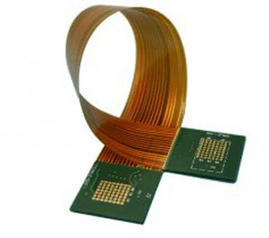
Moreover, design software supports the integration of advanced technologies, such as High-Density Interconnect (HDI) and flexible PCBs.
These technologies are becoming increasingly popular in modern electronics due to their ability to support more complex and compact designs. Design software provides the necessary tools and features to incorporate these technologies into the PCB layout, ensuring that the final product meets the required specifications and performance standards.
In conclusion, the role of design software in streamlining PCB routing is multifaceted and indispensable. By automating routine tasks, enhancing accuracy, facilitating collaboration, enabling simulations, and supporting advanced technologies, design software significantly improves the efficiency and quality of PCB manufacturing. As the demand for more sophisticated and reliable electronic devices continues to grow, the importance of leveraging advanced design software in PCB routing will only become more pronounced.