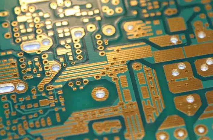
Pcb manufacturing tools
Essential Soldering Tools for PCB Manufacturing
In the realm of printed circuit board (PCB) manufacturing, the precision and reliability of the final product hinge significantly on the tools employed during the soldering process. Soldering, a fundamental step in PCB assembly, involves the joining of electronic components to the board, ensuring both electrical connectivity and mechanical stability. To achieve optimal results, a variety of essential soldering tools are indispensable, each playing a crucial role in the intricate process.
First and foremost, the soldering iron stands as the cornerstone of any soldering toolkit.
This handheld tool, equipped with a heated metal tip, is used to melt solder, allowing it to flow into the joint between the component lead and the PCB pad. Modern soldering irons often feature adjustable temperature controls, enabling precise regulation of heat to suit different soldering tasks. Coupled with the soldering iron, a soldering station provides a stable platform and often includes additional functionalities such as temperature readouts and tip cleaning mechanisms, enhancing the efficiency and accuracy of the soldering process.
Transitioning from the soldering iron, another critical tool is the solder itself.
Solder is a fusible metal alloy, typically composed of tin and lead, although lead-free alternatives are increasingly prevalent due to health and environmental considerations. The choice of solder can significantly impact the quality of the solder joints, with factors such as melting point, flux content, and alloy composition playing pivotal roles. Flux, an integral component of solder, serves to clean and prepare the surfaces to be joined, promoting better adhesion and reducing the likelihood of defects such as cold joints or bridging.
In addition to the soldering iron and solder, desoldering tools are equally essential for PCB manufacturing.
Desoldering pumps, also known as solder suckers, are used to remove excess solder from joints, facilitating the rework or replacement of components. These tools operate by creating a vacuum that draws molten solder away from the joint, ensuring a clean and precise removal. Complementing desoldering pumps, desoldering braid or wick is another effective tool for solder removal. This braided copper wire, when placed over a solder joint and heated, absorbs the molten solder through capillary action, leaving the joint clean and ready for rework.
Furthermore, precision tools such as tweezers and magnifying lamps are indispensable for handling and inspecting small components.
Tweezers allow for the careful placement and adjustment of components on the PCB, while magnifying lamps provide enhanced visibility, enabling the detection of fine details and potential defects. These tools are particularly vital when working with surface-mount technology (SMT) components, which are often minuscule and require meticulous handling.
Moreover, soldering aids such as third hands or PCB holders provide stability and support during the soldering process.
These tools hold the PCB in place, freeing the operator’s hands to focus on the soldering task. This not only improves precision but also reduces the risk of accidental movement or misalignment of components.
In conclusion, the array of essential soldering tools for PCB manufacturing encompasses a diverse range of instruments, each contributing to the overall quality and reliability of the final product. From the fundamental soldering iron and solder to desoldering tools, precision instruments, and supportive aids, each tool plays a vital role in ensuring successful PCB assembly. By understanding and utilizing these tools effectively, manufacturers can achieve high standards of craftsmanship and functionality in their electronic products.
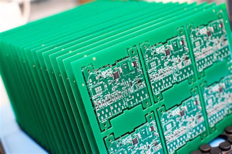
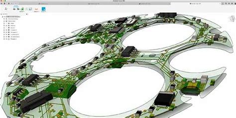
Advanced PCB Design Software for Professionals
In the realm of printed circuit board (PCB) manufacturing, the role of advanced PCB design software cannot be overstated. These sophisticated tools are indispensable for professionals who seek to create intricate and reliable electronic circuits. As the complexity of electronic devices continues to escalate, the demand for robust and feature-rich design software has become paramount. This article delves into the various advanced PCB design software options available to professionals, highlighting their capabilities and the advantages they offer in the PCB manufacturing process.
To begin with, one of the most prominent software tools in the industry is Altium Designer.
Renowned for its comprehensive suite of features, Altium Designer provides an integrated environment that facilitates seamless design, simulation, and verification of PCBs. Its user-friendly interface, coupled with powerful design capabilities, allows engineers to create complex multi-layer boards with ease. Moreover, Altium Designer’s real-time collaboration features enable teams to work concurrently on projects, thereby enhancing productivity and reducing the likelihood of errors.
Transitioning to another notable software, Cadence Allegro stands out for its high-performance design and analysis capabilities.
Cadence Allegro is particularly favored in industries where precision and reliability are critical, such as aerospace and automotive sectors. The software’s advanced routing algorithms and signal integrity analysis tools ensure that the final PCB design meets stringent performance criteria. Additionally, Cadence Allegro’s extensive library of components and materials streamlines the design process, allowing engineers to focus on innovation rather than mundane tasks.
Similarly, Mentor Graphics’ PADS Professional is a powerful tool that caters to both novice and experienced PCB designers.
PADS Professional offers a scalable solution that can grow with the user’s needs, making it an ideal choice for startups and established enterprises alike. The software’s intuitive design environment, coupled with its robust simulation and verification tools, ensures that designs are both functional and manufacturable. Furthermore, PADS Professional’s integration with other Mentor Graphics tools provides a seamless workflow from concept to production.
In addition to these well-known software options, there are other specialized tools that cater to specific aspects of PCB design.
For instance, Zuken’s CR-8000 is a comprehensive design platform that excels in managing the entire product lifecycle. From initial concept through to manufacturing and maintenance, CR-8000 offers a holistic approach to PCB design. Its advanced 3D visualization and co-design capabilities enable engineers to identify potential issues early in the design process, thereby reducing costly rework and delays.
Moreover, Autodesk’s Eagle is another noteworthy mention, particularly for its affordability and ease of use.
While it may not offer the extensive feature set of some of its more expensive counterparts, Eagle is highly regarded for its flexibility and community support. This makes it an excellent choice for small businesses and hobbyists who require a reliable yet cost-effective design solution.
In conclusion, the landscape of advanced PCB design software is rich with options that cater to a wide range of needs and expertise levels. Whether it is the comprehensive capabilities of Altium Designer, the precision of Cadence Allegro, the scalability of PADS Professional, the lifecycle management of Zuken’s CR-8000, or the affordability of Autodesk’s Eagle, professionals have a plethora of tools at their disposal. By leveraging these advanced software solutions, engineers can ensure that their PCB designs are not only innovative but also reliable and manufacturable, thereby meeting the ever-evolving demands of the electronics industry.
Best Practices for Using PCB Drilling Machines
When it comes to the intricate process of printed circuit board (PCB) manufacturing, the use of PCB drilling machines is indispensable. These machines are designed to create precise holes in the PCB substrate, which are essential for mounting components and establishing electrical connections. To ensure optimal performance and longevity of both the drilling machines and the PCBs themselves, it is crucial to adhere to best practices.
First and foremost, selecting the appropriate drill bit is paramount.
The choice of drill bit should be based on the material of the PCB substrate and the required hole diameter. Carbide drill bits are commonly used due to their durability and ability to maintain sharpness over extended periods. However, it is essential to regularly inspect and replace worn-out bits to prevent damage to the PCB and ensure clean, accurate holes.
Equally important is the calibration of the drilling machine.
proper calibration ensures that the drill bit aligns correctly with the designated drilling points on the PCB. Misalignment can lead to off-center holes, which can compromise the functionality of the PCB. Regular maintenance checks and calibration adjustments are necessary to maintain the precision of the drilling process.
In addition to calibration, controlling the drilling speed and feed rate is critical.
High-speed drilling can generate excessive heat, which may cause the PCB material to warp or delaminate. Conversely, a slow feed rate can result in rough hole edges and increased wear on the drill bit. Striking a balance between speed and feed rate, tailored to the specific material and thickness of the PCB, is essential for achieving optimal results.
Another best practice involves the use of backing and entry materials.
These materials are placed above and below the PCB during drilling to support the substrate and prevent burr formation. Backing materials, such as phenolic or aluminum sheets, provide a stable base, while entry materials, like thin aluminum or plastic films, protect the PCB surface from damage. Utilizing these materials can significantly enhance the quality of the drilled holes and extend the life of the drill bits.
Furthermore, maintaining a clean working environment is vital.
Dust and debris generated during the drilling process can accumulate on the PCB surface and within the drilling machine, leading to potential defects and machine malfunctions. Implementing an effective dust extraction system and regularly cleaning the machine and work area can mitigate these issues and ensure a smooth drilling operation.
Monitoring the temperature and humidity levels in the manufacturing environment is also crucial.
Extreme temperatures and humidity fluctuations can affect the PCB material properties and the performance of the drilling machine. Maintaining a controlled environment helps in preserving the integrity of the PCB and the accuracy of the drilling process.
Lastly, operator training and adherence to safety protocols cannot be overstated.
Skilled operators who are well-versed in the operation and maintenance of PCB drilling machines are essential for achieving high-quality results. Comprehensive training programs and strict adherence to safety guidelines help in minimizing the risk of accidents and ensuring a safe and efficient manufacturing process.
In conclusion, the successful use of PCB drilling machines hinges on a combination of proper tool selection, machine calibration, controlled drilling parameters, use of backing and entry materials, cleanliness, environmental control, and operator expertise. By following these best practices, manufacturers can enhance the precision and reliability of their PCB drilling operations, ultimately contributing to the production of high-quality printed circuit boards.
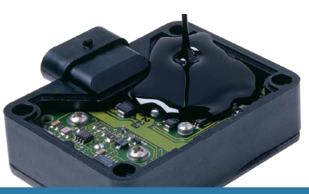
Importance of Reflow Ovens in PCB Assembly
In the realm of printed circuit board (PCB) assembly, the reflow oven stands as a pivotal tool, playing a crucial role in ensuring the reliability and functionality of electronic devices. The importance of reflow ovens in PCB assembly cannot be overstated, as they are instrumental in the soldering process, which is essential for attaching surface mount components to the PCB. This process, known as reflow soldering, involves the application of solder paste to the PCB, placement of components, and subsequent heating in the reflow oven to create strong, reliable solder joints.
To begin with, reflow ovens provide a controlled environment where precise temperature profiles can be maintained.
This is critical because different solder pastes and components have specific thermal requirements. The reflow oven ensures that the PCB is heated uniformly, preventing issues such as cold solder joints or component damage due to excessive heat. By carefully controlling the temperature, reflow ovens help achieve optimal soldering conditions, which directly impacts the performance and longevity of the final product.
Moreover, the reflow oven’s ability to manage temperature profiles is essential for the integrity of the solder joints.
The process typically involves several stages, including preheating, soaking, reflow, and cooling. Each stage has distinct temperature and time requirements that must be meticulously followed. For instance, during the preheating stage, the PCB is gradually heated to avoid thermal shock, which could damage sensitive components. The soaking stage ensures that the entire board reaches a uniform temperature, allowing the flux in the solder paste to activate and clean the surfaces to be soldered. The reflow stage is where the solder paste melts and forms the actual solder joints, and finally, the cooling stage solidifies these joints, ensuring their strength and reliability.
In addition to temperature control, reflow ovens offer the advantage of automation, which enhances the efficiency and consistency of the PCB assembly process.
Automated reflow ovens can handle large volumes of PCBs with minimal human intervention, reducing the likelihood of errors and increasing production throughput. This automation is particularly beneficial in high-volume manufacturing environments, where consistency and speed are paramount. By standardizing the reflow soldering process, manufacturers can achieve higher yields and better quality control, ultimately leading to more reliable electronic products.
Furthermore, reflow ovens contribute to the overall cost-effectiveness of PCB assembly.
While the initial investment in a high-quality reflow oven may be significant, the long-term benefits far outweigh the costs. The precision and reliability offered by reflow ovens reduce the need for rework and repairs, which can be time-consuming and expensive. Additionally, the ability to process multiple PCBs simultaneously increases production efficiency, allowing manufacturers to meet tight deadlines and market demands.
In conclusion, the importance of reflow ovens in PCB assembly is multifaceted, encompassing aspects of temperature control, automation, and cost-effectiveness. These ovens are indispensable for creating reliable solder joints, which are the foundation of any functional electronic device. By providing a controlled environment for the reflow soldering process, reflow ovens ensure that PCBs meet the stringent quality standards required in today’s competitive electronics industry. As technology continues to advance, the role of reflow ovens in PCB assembly will remain critical, underscoring their significance in the production of high-quality electronic products.

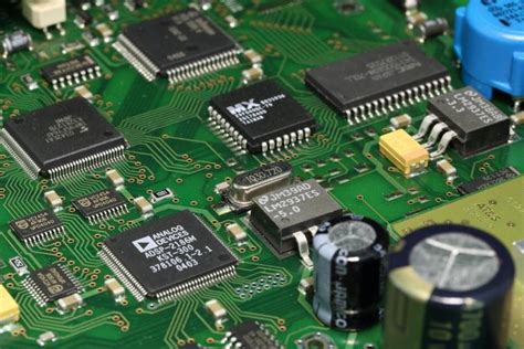
Innovations in PCB Inspection and Testing Equipment
In the rapidly evolving field of electronics, the manufacturing of printed circuit boards (PCBs) has seen significant advancements, particularly in the realm of inspection and testing equipment. These innovations are crucial for ensuring the reliability and performance of PCBs, which are the backbone of modern electronic devices. As the complexity of PCBs increases, so does the need for sophisticated inspection and testing tools that can detect even the minutest of defects and ensure optimal functionality.
One of the most notable advancements in PCB inspection is the development of automated optical inspection (AOI) systems.
AOI technology utilizes high-resolution cameras and advanced algorithms to meticulously scan PCBs for defects such as soldering issues, component misalignments, and surface irregularities. The precision of AOI systems allows for the detection of defects that might be missed by manual inspection, thereby significantly reducing the risk of faulty PCBs reaching the market. Moreover, the integration of machine learning and artificial intelligence into AOI systems has further enhanced their accuracy and efficiency, enabling them to learn from previous inspections and continuously improve their defect detection capabilities.
In addition to AOI, X-ray inspection systems have become indispensable in the PCB manufacturing process.
These systems provide a non-destructive means of examining the internal structures of PCBs, including solder joints and hidden connections that are not visible to the naked eye. By using X-ray technology, manufacturers can identify defects such as voids, cracks, and misalignments within the layers of the PCB. This level of scrutiny is particularly important for high-density interconnect (HDI) PCBs, which have multiple layers and complex architectures. The ability to inspect these intricate designs without causing damage is a significant advantage, ensuring that only the highest quality PCBs are produced.
Transitioning from inspection to testing, in-circuit testing (ICT) remains a cornerstone of PCB quality assurance.
ICT involves the use of a bed-of-nails fixture to make electrical contact with various test points on the PCB. This method allows for the verification of electrical connections, component values, and functionality. Recent innovations in ICT have focused on improving the speed and accuracy of testing, as well as reducing the physical footprint of the testing equipment. For instance, advancements in fixture design and the use of modular test systems have made ICT more adaptable to different PCB designs and production volumes.
Another significant development in PCB testing is the adoption of boundary scan technology, also known as JTAG (Joint Test Action Group).
Boundary scan testing allows for the testing of PCBs without the need for physical test probes, making it ideal for densely populated boards where traditional ICT may not be feasible. By leveraging the built-in test capabilities of modern integrated circuits, boundary scan technology can perform comprehensive tests on the interconnections and components of a PCB. This method not only enhances test coverage but also simplifies the testing process, reducing the time and cost associated with PCB testing.
Furthermore, functional testing has seen improvements with the integration of automated test equipment (ATE).
ATE systems are designed to simulate the operational environment of the PCB, testing its performance under real-world conditions. These systems can execute a wide range of tests, from simple continuity checks to complex functional tests that mimic the PCB’s intended use. The automation of these tests ensures consistency and repeatability, providing manufacturers with reliable data on the performance of their PCBs.
In conclusion, the innovations in PCB inspection and testing equipment have significantly enhanced the quality and reliability of PCBs. From advanced AOI and X-ray inspection systems to improved ICT, boundary scan technology, and automated functional testing, these tools are essential for meeting the stringent demands of modern electronics manufacturing. As technology continues to advance, we can expect further improvements in these areas