PCB Module Fanout Design Guide
Introduction
Printed Circuit Board (PCB) design involves multiple critical steps, one of which is fanout design—the process of routing traces from component pads to vias or other layers. Proper fanout ensures signal integrity, thermal management, manufacturability, and electromagnetic compatibility (EMC).
This guide explores PCB module fanout design principles, best practices, and common techniques to optimize performance in high-speed, high-density, and mixed-signal designs.
1. Understanding Fanout in PCB Design
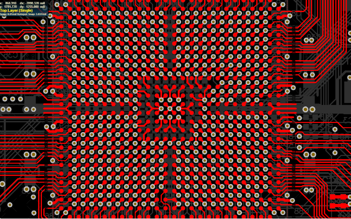
Fanout refers to the method of connecting surface-mount device (SMD) pads to vias or traces that distribute signals across different PCB layers. It is especially crucial for:
- Ball Grid Array (BGA) packages
- QFN (Quad Flat No-Lead) and LGA (Land Grid Array) packages
- High-pin-count connectors
Key Objectives of Fanout Design
- Signal Integrity (SI): Minimize impedance mismatches and reflections.
- Power Delivery: Ensure low-impedance power distribution.
- Thermal Management: Facilitate heat dissipation through vias.
- Manufacturability: Avoid manufacturing defects like solder bridging or incomplete etching.
2. Fanout Design Rules and Best Practices
2.1 Via Selection and Placement
- Via Types:
- Through-hole vias: Standard for most designs.
- Blind/Buried vias: Used in HDI (High-Density Interconnect) PCBs.
- Microvias: Essential for fine-pitch BGAs (e.g., 0.5mm pitch or smaller).
- Via Placement Guidelines:
- Place vias as close to the pad as possible without violating DFM (Design for Manufacturing) rules.
- For BGAs, use dog-bone fanout (a short trace connecting the pad to the via).
- Avoid placing vias in solder mask-defined (SMD) pads unless necessary (may cause solder wicking issues).
2.2 Trace Width and Spacing
- Follow IPC-2221/7351 standards for trace width based on current requirements.
- Maintain consistent impedance for high-speed signals (e.g., 50Ω for single-ended, 100Ω for differential pairs).
- Use teardrops to strengthen connections between traces and pads/vias.
2.3 Escape Routing Strategies
- BGA Fanout Techniques:
- Staggered Fanout: Alternate via placement to maximize routing channels.
- Via-in-Pad: Directly place a via in the pad (requires plating and filling).
- Differential Pair Fanout: Maintain tight coupling during escape routing.
- QFN/LGA Fanout:
- Use perimeter fanout for thermal pads.
- Ensure symmetrical via placement for power/ground connections.
2.4 Power and Ground Fanout
- Use multiple vias for power/ground connections to reduce inductance.
- Implement solid copper pours with stitching vias for low-impedance return paths.
- Avoid split planes under high-speed signals to prevent discontinuities.

3. High-Speed Signal Fanout Considerations
3.1 Impedance Control
- Match trace impedance to the driver/receiver specifications.
- Minimize via stubs (use back-drilling if necessary).
3.2 Crosstalk Mitigation
- Maintain 3W rule (trace spacing ≥ 3× trace width) for critical signals.
- Use ground shielding between sensitive traces.
3.3 Length Matching
- Apply serpentine routing for timing-critical signals (e.g., DDR, PCIe).
- Ensure matched via counts for differential pairs.
4. Thermal and Power Integrity in Fanout Design
4.1 Thermal Vias
- Place thermal vias under hot components (e.g., processors, FPGAs).
- Use filled and capped vias for better heat conduction.
4.2 Power Distribution Network (PDN) Optimization
- Implement low-inductance fanout with multiple vias per power pin.
- Use decoupling capacitors near IC power pins.
5. Manufacturing and DFM Considerations
5.1 Solder Mask and Via Plugging
- Use solder mask dams to prevent solder migration.
- For via-in-pad, specify via filling (conductive/non-conductive).
5.2 Drill-to-Copper Clearance
- Follow fabricator capabilities (typically ≥ 8mil annular ring).
- Avoid copper slivers that may etch away during fabrication.
5.3 Panelization and Breakaway Tabs
- Ensure fanout does not interfere with PCB depaneling.

6. Common Fanout Mistakes and How to Avoid Them
| Mistake | Solution |
|---|---|
| Insufficient via count for power pins | Add multiple vias per power/ground connection |
| Long stub vias degrading signal integrity | Use blind vias or back-drilling |
| Uneven via distribution causing warpage | Balance via placement across the PCB |
| Poor thermal via placement leading to overheating | Add thermal vias under high-power components |
7. Tools and Software for Fanout Design
- Cadence Allegro (Auto-interactive fanout)
- Altium Designer (Via stitching tools)
- Mentor Xpedition (HDI fanout support)
- KiCad (Open-source fanout utilities)
Conclusion
Effective PCB fanout design is critical for signal integrity, power delivery, and manufacturability. By following structured fanout strategies—such as proper via placement, impedance control, and thermal management—designers can optimize performance in complex PCB modules.
Always collaborate with PCB manufacturers to validate design rules and leverage automated fanout tools to streamline the process. With careful planning, fanout design can significantly enhance PCB reliability and functionality.