PCB Motherboard Design: A Comprehensive Guide
Introduction
Printed Circuit Board (PCB) motherboard design is a critical aspect of modern electronics. The motherboard, often referred to as the mainboard or system board, is the backbone of any electronic device, providing the necessary connections and pathways for various components to communicate and function together. This article delves into the intricacies of PCB motherboard design, covering the fundamental principles, design considerations, and best practices.
1. Understanding the Basics of PCB Motherboard Design
1.1 What is a PCB Motherboard?
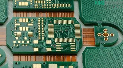
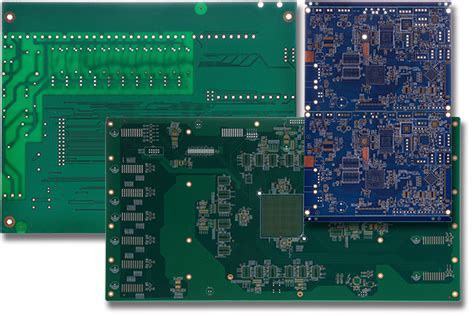
A PCB motherboard is a multi-layered board that houses the primary components of an electronic device, such as the CPU, memory, storage, and peripheral connectors. It serves as the central hub that facilitates communication between these components, ensuring the device operates efficiently.
1.2 Key Components of a PCB Motherboard
- CPU Socket: The central processing unit (CPU) is the brain of the computer, and the socket is where it is installed.
- Memory Slots: These slots hold the RAM (Random Access Memory) modules, which are crucial for temporary data storage and quick access.
- Expansion Slots: These slots allow for additional components like graphics cards, sound cards, and network cards to be added.
- Power Connectors: These connectors supply power to the motherboard and its components.
- Chipset: The chipset manages data flow between the CPU, memory, and peripherals.
- BIOS/UEFI Chip: This chip contains the firmware that initializes the hardware during the boot process.
- Connectors: Various connectors for USB, HDMI, audio, and other peripherals are integrated into the motherboard.
2. Design Considerations for PCB Motherboards
2.1 Layer Stackup
The layer stackup is a critical aspect of PCB motherboard design. It determines the number of layers and their arrangement, which affects the board’s performance, signal integrity, and manufacturability.
- Signal Layers: These layers carry electrical signals between components. High-speed signals require careful routing to minimize interference and signal loss.
- Power and Ground Layers: These layers distribute power and provide a reference ground for the circuit. Proper design ensures stable power delivery and reduces noise.
- Dielectric Material: The material between layers affects the board’s electrical properties. Common materials include FR-4, Rogers, and polyimide.
2.2 Signal Integrity
Signal integrity is paramount in PCB motherboard design, especially for high-speed signals. Factors to consider include:
- Impedance Matching: Ensuring that the impedance of the transmission lines matches the source and load impedances to prevent signal reflections.
- Crosstalk: Minimizing crosstalk between adjacent signal traces by maintaining adequate spacing and using ground planes.
- Signal Loss: Reducing signal loss by using appropriate trace widths, materials, and routing techniques.
2.3 Power Integrity
Power integrity ensures that the motherboard receives stable and clean power. Key considerations include:
- Decoupling Capacitors: Placing decoupling capacitors near power pins to filter out noise and stabilize voltage.
- Power Plane Design: Designing power planes to minimize voltage drops and ensure even power distribution.
- Voltage Regulation: Using voltage regulators to maintain consistent voltage levels for different components.
2.4 Thermal Management
Thermal management is crucial to prevent overheating and ensure reliable operation. Design strategies include:
- Heat Sinks: Attaching heat sinks to high-power components like the CPU and voltage regulators.
- Thermal Vias: Using thermal vias to conduct heat away from critical components.
- Airflow: Designing the board layout to facilitate airflow and cooling.
2.5 Manufacturability and Assembly
Designing for manufacturability (DFM) ensures that the motherboard can be efficiently and reliably produced. Considerations include:
- Component Placement: Arranging components to minimize trace lengths and simplify assembly.
- Test Points: Including test points for easier debugging and testing during manufacturing.
- Panelization: Designing the board to fit standard panel sizes for efficient production.
3. Design Process for PCB Motherboards
3.1 Schematic Design
The schematic design is the first step in the PCB design process. It involves creating a graphical representation of the circuit, showing how components are connected.
- Component Selection: Choosing the right components based on performance, cost, and availability.
- Netlist Generation: Creating a netlist that defines the electrical connections between components.
- Simulation: Running simulations to verify the circuit’s functionality and performance.
3.2 PCB Layout
The PCB layout involves placing components and routing traces on the board. Key steps include:
- Component Placement: Positioning components to optimize signal paths, thermal management, and manufacturability.
- Routing: Connecting components with traces while adhering to design rules for signal integrity and power integrity.
- Design Rule Check (DRC): Running a DRC to ensure the layout complies with manufacturing and design constraints.
3.3 Design Verification
Design verification ensures that the PCB meets all functional and performance requirements. Techniques include:
- Signal Integrity Analysis: Analyzing signal paths to identify and mitigate issues like crosstalk and reflections.
- Power Integrity Analysis: Verifying that power delivery is stable and meets the requirements of all components.
- Thermal Analysis: Simulating thermal performance to identify potential hotspots and optimize cooling.
3.4 Prototyping and Testing
Prototyping and testing are essential to validate the design before mass production. Steps include:
- Prototype Fabrication: Producing a small batch of boards for testing.
- Functional Testing: Verifying that the board operates as intended.
- Debugging: Identifying and fixing any issues discovered during testing.
4. Advanced Topics in PCB Motherboard Design
4.1 High-Speed Design
High-speed design is critical for modern motherboards, which often operate at GHz frequencies. Key considerations include:
- Differential Pair Routing: Routing high-speed signals as differential pairs to reduce noise and improve signal integrity.
- Length Matching: Ensuring that signal paths are of equal length to prevent timing skew.
- Via Optimization: Minimizing the use of vias and optimizing their placement to reduce signal loss and reflections.
4.2 EMI/EMC Considerations
Electromagnetic interference (EMI) and electromagnetic compatibility (EMC) are important factors in PCB design. Strategies to mitigate EMI/EMC issues include:
- Shielding: Using shielding techniques to contain electromagnetic radiation.
- Grounding: Implementing proper grounding practices to reduce noise and interference.
- Filtering: Adding filters to suppress unwanted frequencies and reduce EMI.
4.3 Flexible and Rigid-Flex PCBs
Flexible and rigid-flex PCBs offer unique advantages for certain applications. Design considerations include:
- Material Selection: Choosing flexible materials that can withstand bending and flexing.
- Layer Stackup: Designing a stackup that accommodates both rigid and flexible sections.
- Routing: Routing traces to minimize stress and prevent cracking in flexible areas.
4.4 Design for Reliability (DFR)
Design for reliability (DFR) focuses on ensuring the long-term reliability of the motherboard. Techniques include:
- Redundancy: Adding redundant components or pathways to improve fault tolerance.
- Stress Testing: Subjecting the board to stress tests to identify potential failure points.
- Environmental Considerations: Designing the board to withstand environmental factors like temperature, humidity, and vibration.
5. Tools and Software for PCB Motherboard Design
5.1 CAD Tools
Computer-aided design (CAD) tools are essential for PCB design. Popular tools include:
- Altium Designer: A comprehensive PCB design tool with advanced features for schematic capture, layout, and simulation.
- Cadence Allegro: A powerful tool for high-speed PCB design, offering robust signal integrity and power integrity analysis.
- KiCad: An open-source PCB design tool that provides a complete suite for schematic capture and PCB layout.
5.2 Simulation Tools
Simulation tools help verify the design before prototyping. Commonly used tools include:
- SPICE: A general-purpose circuit simulation program used for analog and mixed-signal circuits.
- HyperLynx: A signal integrity and power integrity analysis tool integrated with many CAD platforms.
- ANSYS HFSS: A high-frequency structure simulator used for electromagnetic simulation and analysis.
5.3 DFM Tools
Design for manufacturability (DFM) tools ensure that the design can be efficiently produced. Examples include:
- Valor NPI: A DFM tool that checks for manufacturability issues and provides recommendations for improvement.
- Mentor Xpedition: A tool that offers DFM analysis and optimization for PCB designs.
6. Future Trends in PCB Motherboard Design
6.1 Miniaturization
As electronic devices become smaller and more compact, PCB motherboards must also shrink in size. This trend drives the need for advanced packaging techniques, such as system-in-package (SiP) and chip-on-board (CoB).
6.2 High-Density Interconnect (HDI)
HDI technology allows for more components and connections in a smaller area. This is achieved through the use of microvias, fine-pitch components, and advanced routing techniques.
6.3 Integration of Advanced Materials
The use of advanced materials, such as low-loss dielectrics and high-conductivity metals, is becoming more common. These materials improve performance and enable higher-frequency operation.
6.4 AI and Machine Learning in Design
Artificial intelligence (AI) and machine learning (ML) are increasingly being used to optimize PCB designs. These technologies can automate tasks like component placement, routing, and signal integrity analysis, leading to faster and more efficient design processes.
Conclusion
PCB motherboard design is a complex and multifaceted process that requires a deep understanding of electronics, materials, and manufacturing techniques. By considering factors like signal integrity, power integrity, thermal management, and manufacturability, designers can create reliable and high-performance motherboards that meet the demands of modern electronic devices. As technology continues to evolve, staying abreast of the latest trends and tools will be essential for success in this field.


