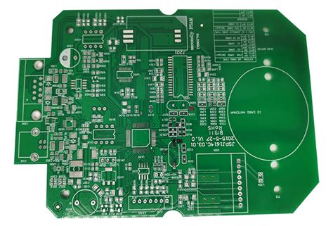
PCB Pad Design: A Comprehensive Guide to Optimizing Performance and Manufacturability
The design of PCB (Printed Circuit Board) pads is a critical aspect of PCB layout that directly impacts the solderability, reliability, and manufacturability of electronic assemblies. Pads are the exposed metal areas on a PCB where components are soldered, and their design must account for factors such as component type, soldering process, thermal management, and mechanical stability. Poor pad design can lead to soldering defects, electrical failures, and reduced product lifespan. This article provides a comprehensive guide to PCB pad design, covering key principles, types of pads, design considerations, and best practices to ensure optimal performance and manufacturability.
1. Introduction to PCB Pad Design
PCB pads serve as the interface between components and the PCB, providing both electrical connections and mechanical support. The design of these pads must balance electrical performance, thermal management, and manufacturability. Key factors influencing pad design include:
- Component Type: Different components, such as surface-mount devices (SMDs) and through-hole components, require specific pad geometries.
- Soldering Process: The choice of soldering method (e.g., reflow, wave, or hand soldering) affects pad size, shape, and spacing.
- Thermal Considerations: Pads must dissipate heat effectively to prevent thermal stress and ensure reliable solder joints.
- Mechanical Stability: Pads must provide sufficient mechanical strength to withstand mechanical stress and vibration.
2. Types of PCB Pads
2.1 Surface-Mount Device (SMD) Pads
SMD pads are designed for components that are mounted directly onto the surface of the PCB. Common SMD pad types include:
- Rectangular Pads: Used for passive components like resistors and capacitors.
- Circular or Oval Pads: Used for larger components, such as integrated circuits (ICs) or connectors.
- Thermal Pads: Used for components that generate significant heat, such as power transistors or voltage regulators. These pads often include thermal vias to improve heat dissipation.
2.2 Through-Hole Pads
Through-hole pads are designed for components with leads that pass through holes in the PCB. These pads typically include a plated through-hole (PTH) for soldering. Common through-hole pad types include:
- Annular Rings: The copper area surrounding the drilled hole. The size of the annular ring must be sufficient to ensure a reliable solder joint.
- Thermal Relief Pads: Used to reduce thermal mass and improve soldering for through-hole components. These pads have spokes connecting the pad to the copper plane, allowing for better heat distribution.
2.3 Ball Grid Array (BGA) Pads
BGA pads are used for components with an array of solder balls on their underside. These pads are typically circular and must be precisely aligned with the solder balls.
- Solder Mask Defined (SMD): The solder mask defines the pad size, leaving a smaller exposed copper area.
- Non-Solder Mask Defined (NSMD): The copper defines the pad size, providing better mechanical strength.
2.4 Test Pads
Test pads are used for testing and debugging purposes. They are typically small, exposed copper areas that allow probes to make electrical contact with the circuit.
3. Key Considerations for PCB Pad Design
3.1 Component Footprint
The pad design must match the component footprint specified in the datasheet. Key parameters include:
- Pad Size: The pad should be slightly larger than the component lead or solder ball to ensure proper soldering.
- Pad Shape: The shape of the pad should match the component lead or solder ball (e.g., rectangular for SMD resistors, circular for BGA balls).
- Pad Spacing: The spacing between pads must match the component lead pitch to avoid short circuits or open connections.
3.2 Soldering Process
The choice of soldering method affects pad design. Key considerations include:
- Reflow Soldering: Pads must be designed to accommodate solder paste deposition and reflow profiles.
- Wave Soldering: Pads must be designed to prevent solder bridging and ensure proper solder fillets.
- Hand Soldering: Pads must be large enough to allow manual soldering and inspection.
3.3 Thermal Management
Thermal considerations are critical for components that generate significant heat. Key strategies include:
- Thermal Vias: Use thermal vias under pads to transfer heat to the inner layers or the opposite side of the PCB.
- Copper Pour: Increase the copper area around pads to improve heat dissipation.
- Thermal Relief Pads: Use thermal relief pads for through-hole components to reduce thermal mass and improve soldering.
3.4 Mechanical Stability
Pads must provide sufficient mechanical strength to withstand mechanical stress and vibration. Key considerations include:
- Pad Size: Larger pads provide better mechanical stability but may increase the risk of solder bridging.
- Anchoring: Use additional copper features, such as teardrops or anchors, to strengthen the connection between pads and traces.
3.5 Solder Mask and Paste Mask
The solder mask and paste mask play a critical role in pad design. Key considerations include:
- Solder Mask Clearance: Ensure adequate clearance between the solder mask and the pad to prevent solder mask encroachment.
- Paste Mask Aperture: Design the paste mask aperture to match the pad size and shape, ensuring proper solder paste deposition.
4. Best Practices for PCB Pad Design
4.1 Follow Manufacturer Guidelines
Always refer to the component manufacturer’s datasheet for recommended pad dimensions and spacing. Deviating from these guidelines can lead to soldering defects or reliability issues.
4.2 Use Standard Footprints
Use standard footprints from component libraries to ensure consistency and reduce the risk of errors. Custom footprints should only be used when necessary.
4.3 Optimize Pad Size and Shape
- SMD Pads: Ensure the pad size is slightly larger than the component lead to allow for proper solder fillets.
- Through-Hole Pads: Ensure the annular ring is sufficiently large to provide a reliable solder joint.
- BGA Pads: Use precise pad sizes and spacing to match the solder ball array.
4.4 Implement Thermal Management
- Thermal Vias: Place thermal vias under pads for heat-generating components to improve heat dissipation.
- Copper Pour: Use copper pours around pads to enhance thermal performance.
4.5 Ensure Mechanical Stability
- Teardrops: Use teardrops to strengthen the connection between pads and traces.
- Anchors: Add anchors or additional copper features to improve mechanical stability.
4.6 Test and Validate
- Prototype Testing: Build and test prototypes to validate pad design and soldering performance.
- Inspection: Use visual inspection and automated optical inspection (AOI) to identify soldering defects.
5. Common Challenges and Solutions
5.1 Solder Bridging
- Challenge: Solder bridging occurs when solder connects adjacent pads, causing short circuits.
- Solution: Increase pad spacing, reduce pad size, or adjust solder paste deposition.
5.2 Tombstoning
- Challenge: Tombstoning occurs when one end of a surface-mount component lifts off the pad during soldering.
- Solution: Ensure symmetrical pad design and uniform heating during reflow.
5.3 Poor Solder Joints
- Challenge: Poor solder joints can result from insufficient pad size or improper soldering.
- Solution: Optimize pad size, shape, and solder paste deposition.
6. Emerging Trends in PCB Pad Design
6.1 Miniaturization
The trend toward smaller and more compact devices is driving the need for smaller pads and finer pitch components.
6.2 Advanced Materials
New materials, such as high-temperature laminates and low-loss dielectrics, are being used to improve pad performance.
6.3 Additive Manufacturing
Additive manufacturing techniques, such as 3D printing, are being explored for creating custom pad geometries and prototypes.
7. Conclusion
PCB pad design is a critical aspect of PCB layout that directly impacts the performance, reliability, and manufacturability of electronic assemblies. By following best practices for pad size, shape, spacing, and thermal management, designers can ensure robust solder joints and reliable electrical connections. Emerging trends, such as miniaturization and advanced materials, are shaping the future of PCB pad design, offering new opportunities for innovation and performance enhancement. With careful attention to detail and adherence to industry standards, PCB pad design can be optimized to meet the demands of modern electronics.


