PCB Panelization: A Comprehensive Guide to Design, Benefits, and Best Practices
Introduction to PCB Panelization
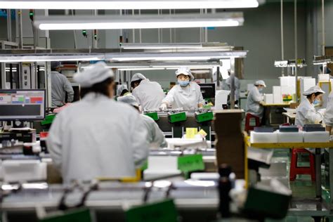
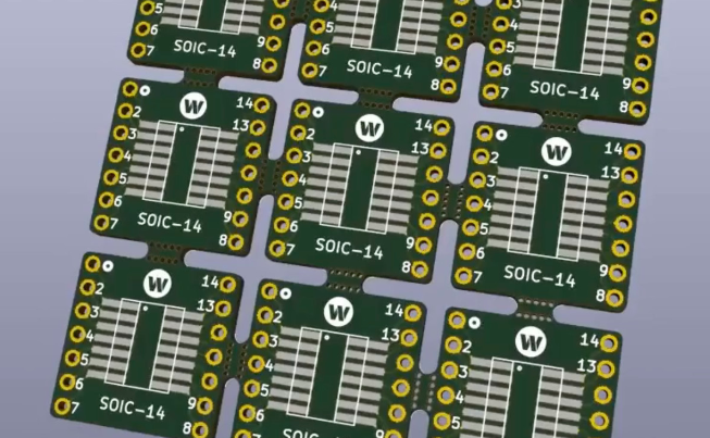
Printed Circuit Board (PCB) panelization is a critical manufacturing technique that involves arranging multiple PCB designs onto a single panel for production. This process has become an industry standard for optimizing manufacturing efficiency, reducing costs, and improving overall production quality in the electronics industry.
Panelization allows manufacturers to produce dozens or even hundreds of individual PCBs simultaneously on a single substrate, significantly streamlining the assembly process. The practice is particularly valuable for small to medium-sized boards, where individual processing would be impractical and cost-prohibitive.
Understanding PCB Panel Basics
What is a PCB Panel?
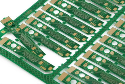
A PCB panel (or array) refers to a larger board that contains multiple instances of the same PCB design or different PCB designs arranged together. These individual PCBs are typically separated after the assembly process through routing, scoring, or breaking along pre-defined lines.
Standard Panel Sizes
Manufacturers typically work with standardized panel sizes to maximize equipment compatibility and production efficiency. Common panel sizes include:
- 18″ × 24″ (457mm × 610mm)
- 21″ × 24″ (533mm × 610mm)
- 18″ × 12″ (457mm × 305mm)
The choice of panel size depends on the manufacturer’s equipment capabilities and the specific requirements of the PCB designs being produced.
Benefits of PCB Panelization
1. Manufacturing Efficiency
Panelization dramatically increases production throughput by allowing multiple boards to be processed simultaneously during:
- Solder paste application
- Component placement
- Reflow soldering
- Wave soldering (for through-hole components)
- Automated optical inspection (AOI)
2. Cost Reduction
By maximizing the use of materials and minimizing handling time, panelization offers significant cost advantages:
- Reduced material waste
- Lower labor costs per unit
- Optimized machine time
- Economies of scale in component purchasing
3. Improved Handling and Assembly
Small PCBs can be difficult to handle individually during assembly. Panelization:
- Provides better mechanical support for fragile boards
- Enables automated handling throughout the assembly process
- Reduces the risk of damage during transportation
4. Consistent Quality
Processing multiple boards simultaneously ensures more consistent:
- Solder paste application
- Component placement accuracy
- Soldering quality across all units
PCB Panelization Methods
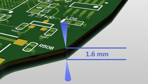
1. V-Scoring (V-Groove)
V-scoring involves creating shallow V-shaped grooves on both sides of the panel along the separation lines. This method:
- Is cost-effective and space-efficient
- Leaves minimal material between boards
- Allows for easy separation after assembly
- Is ideal for rectangular boards with straight edges
2. Tab Routing
Tab routing uses small tabs of material to hold boards in place within the panel. Characteristics include:
- Suitable for irregular board shapes
- Requires breakaway tabs or mouse bites (small perforations)
- May need manual depanelization
- Leaves small protrusions that may require cleaning
3. Perforated Tab Routing
A combination of routing and perforations that:
- Provides more secure holding than standard tabs
- Allows for easier separation than solid tabs
- Reduces stress on components during separation
4. Solid Tab (No Routing)
Boards are connected with solid material bridges that require:
- Saw cutting for separation
- More precise depanelization equipment
- Careful handling to prevent board damage
Design Considerations for PCB Panelization
1. Panel Layout Optimization
Effective panel design requires careful consideration of:
- Board orientation (to maximize quantity per panel)
- Spacing between boards (typically 2-5mm)
- Fiducial markers placement
- Tooling holes for alignment
- Clearance for routing paths
2. Breakaway Tabs Design
When using tab routing, important factors include:
- Tab width (typically 3-5mm)
- Number of tabs per side (usually 3-5)
- Tab location (avoiding sensitive components)
- Mouse bite size and spacing
3. Component Clearance
Critical areas to consider:
- 5mm clearance from board edges for V-scoring
- 3mm clearance from routing paths
- Additional clearance for components near separation lines
4. Fiducial Markers and Tooling
Essential panel features include:
- Global fiducials for the entire panel
- Local fiducials for individual boards (if needed)
- Tooling holes for precise alignment during assembly
- Clearance areas for clamping and handling
Advanced Panelization Techniques
1. Mixed Panelization
Combining different PCB designs in one panel requires:
- Careful planning of assembly processes
- Consideration of different thermal profiles
- Proper documentation for assembly houses
2. Step-and-Repeat Panelization
For high-volume production of identical boards:
- Optimizes material usage
- Simplifies assembly programming
- Ensures consistent quality across all units
3. Flexible PCB Panelization
Special considerations for flex and rigid-flex PCBs:
- Different handling requirements
- Specialized routing techniques
- Unique stress relief requirements
Depanelization Methods
1. Manual Breaking
Suitable for V-scored panels:
- Low-cost method
- Requires careful handling
- May cause some stress to components
2. Pizza Cutter (V-Score Separator)
Specialized tool for:
- Clean separation along V-grooves
- Reduced stress on components
- Consistent break quality
3. Routing Depanelization
Uses CNC routers for:
- Precise separation
- Complex board shapes
- Minimal stress to components
4. Laser Depanelization
High-precision method that:
- Eliminates mechanical stress
- Enables extremely fine cuts
- Is suitable for delicate components
Quality Control in Panelized PCBs
1. Panel-Level Inspection
Critical checks include:
- Dimensional accuracy of the entire panel
- Proper scoring or routing depth
- Fiducial marker quality
- Tooling hole alignment
2. Post-Assembly Verification
Important quality measures:
- Visual inspection of separation edges
- Checking for delamination or damage
- Verifying component integrity near edges
- Testing electrical continuity
Common Panelization Mistakes to Avoid
1. Insufficient Clearance
Problems caused by:
- Components too close to board edges
- Inadequate spacing between boards
- Poor tab placement
2. Improper Tab Design
Issues including:
- Too few tabs causing instability
- Overly strong tabs making separation difficult
- Tabs placed in high-stress areas
3. Ignoring Manufacturer Capabilities
Failure to consider:
- Minimum/maximum panel sizes
- Equipment limitations
- Preferred panelization methods
4. Neglecting Depanelization Requirements
Overlooking:
- Required separation method
- Stress on components during separation
- Post-separation cleaning needs
Future Trends in PCB Panelization
1. Smart Panelization Software
Emerging technologies include:
- AI-powered layout optimization
- Automated design rule checking
- Integration with full PCB design flow
2. Advanced Depanelization Techniques
Innovations such as:
- Improved laser cutting systems
- Vision-guided robotic separation
- Stress-free cutting methods
3. Sustainable Panelization
Eco-friendly developments:
- Optimized material usage algorithms
- Waste reduction techniques
- Recyclable panel materials
Conclusion
PCB panelization remains an essential process in modern electronics manufacturing, offering significant advantages in efficiency, cost reduction, and quality control. As boards become more complex and components more miniaturized, proper panelization techniques grow increasingly important.
By understanding the various panelization methods, design considerations, and best practices outlined in this guide, engineers and designers can optimize their PCB designs for manufacturing while avoiding common pitfalls. The continued evolution of panelization technologies promises to further enhance the benefits of this critical manufacturing process in the years to come.
Effective panelization requires close collaboration between designers and manufacturers to ensure all requirements are met while maximizing production efficiency. As the electronics industry advances, panelization will remain a cornerstone of cost-effective, high-quality PCB manufacturing.