PCB/PCBA Design and Manufacturing Essentials

Key Takeaways
Successful PCB assembly and PCBA development rely on balancing technical precision with practical manufacturing considerations. A well-optimized design begins with understanding signal integrity and thermal management, ensuring layouts minimize interference while maximizing heat dissipation. For high-performance PCBA, component placement and routing strategies must prioritize electrical efficiency and mechanical stability, particularly in dense or high-frequency applications.
Material selection plays a pivotal role in PCB reliability—choosing substrates with appropriate glass transition temperatures (Tg) and copper weights can prevent delamination and improve longevity in harsh environments. Additionally, aligning design specifications with manufacturing capabilities reduces errors during PCB assembly, such as solder bridging or misaligned components.
Tip: Implement design-for-manufacturing (DFM) checks early to identify potential issues like insufficient clearances or unrealistic pad sizes, significantly reducing rework costs.
Testing protocols, including automated optical inspection (AOI) and in-circuit testing (ICT), are critical for validating PCBA functionality and catching defects before mass production. Cost-effective practices, such as panelization for batch processing or standardizing component footprints, streamline scalability without compromising quality.
Emerging trends like embedded components and flexible hybrid electronics are reshaping PCB/PCBA innovation, offering compact and adaptable solutions for modern devices. By integrating these advancements with rigorous quality assurance, manufacturers can deliver robust, efficient, and future-ready electronic systems.
Fundamentals of PCB Design and Layout Optimization
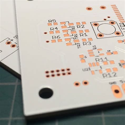
Effective PCB design and layout optimization form the backbone of reliable electronic systems, directly influencing performance, manufacturability, and longevity. A well-optimized layout begins with strategic component placement, ensuring minimal signal interference and efficient thermal management. Critical traces, such as high-speed signal paths or power delivery networks, require careful routing to mitigate electromagnetic interference (EMI) and maintain signal integrity. Utilizing advanced design software enables engineers to simulate and validate layouts before moving to the PCBA phase, reducing costly revisions during PCB assembly.
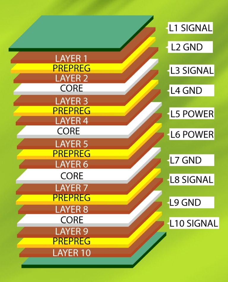
Key considerations include optimizing layer stack-up configurations to balance cost and functionality, particularly in multilayer boards. Proper via placement and sizing are essential to avoid impedance mismatches and ensure robust connections. For high-performance PCBA applications, incorporating Design for Manufacturability (DFM) principles streamlines the transition from design to production, minimizing errors in solder mask application or component misalignment. Additionally, thermal relief patterns and copper balancing prevent warping during reflow soldering, enhancing the reliability of the final product.
Designers must also account for mechanical constraints, such as board size and mounting points, to ensure compatibility with enclosures and end-use environments. By prioritizing these fundamentals, engineers achieve layouts that not only meet electrical requirements but also align with efficient PCB assembly workflows, ultimately delivering cost-effective and scalable solutions for modern electronics.
Key Considerations for High-Performance PCBA Development
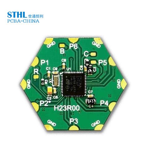
Achieving high-performance PCBA (Printed Circuit Board Assembly) requires balancing design precision, material robustness, and manufacturing expertise. A critical starting point is optimizing PCB assembly processes to ensure seamless integration of components while minimizing signal interference and thermal inefficiencies. Component selection plays a pivotal role—high-reliability parts with appropriate tolerances and temperature ratings are essential for applications in harsh environments or mission-critical systems. Advanced PCB assembly techniques, such as surface-mount technology (SMT), enable tighter component placement, improving signal integrity and reducing parasitic capacitance.
Thermal management must be addressed early in the design phase. Proper heat dissipation strategies, including thermal vias, heatsinks, or copper pours, prevent overheating and extend the lifespan of the PCBA. Similarly, signal integrity demands careful routing of high-speed traces, impedance matching, and minimizing electromagnetic interference (EMI) through shielding or grounding practices. For multi-layer boards, stack-up configuration and dielectric material choices directly impact performance in high-frequency applications.
Collaboration between design and manufacturing teams ensures design for manufacturability (DFM) principles are applied. This includes adhering to clearance rules, avoiding component crowding, and selecting solder mask materials compatible with automated PCB assembly workflows. Testing protocols, such as automated optical inspection (AOI) and X-ray inspection, should be integrated to detect soldering defects or misalignments early.
Cost-effectiveness remains vital without compromising quality. Leveraging standardized PCBA processes, such as panelization for bulk production, reduces waste and accelerates timelines. Finally, incorporating scalable design practices—modular layouts, reusable footprints, and future-proofed interfaces—ensures adaptability to evolving technological demands while maintaining performance benchmarks.
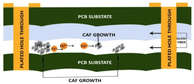
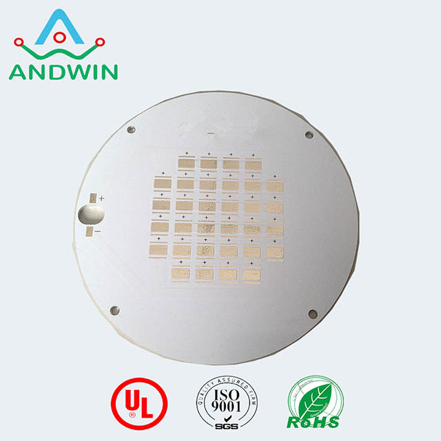
Material Selection Strategies for Enhanced PCB Reliability
Selecting appropriate materials is pivotal for ensuring the long-term reliability of PCB assembly (PCBA) and overall electronic system performance. The choice of substrate, copper layers, and solder mask directly impacts thermal management, signal integrity, and mechanical durability. For high-frequency or high-power applications, materials like FR-4, polyimide, or Rogers laminates are commonly evaluated based on their dielectric constants, thermal conductivity, and moisture absorption rates. For instance, PCBA designs requiring extended thermal cycling resilience often benefit from substrates with a high glass transition temperature (Tg), which minimizes warping under temperature fluctuations.
Copper weight and trace thickness must align with current-carrying requirements to prevent overheating, while advanced solder mask formulations enhance resistance to environmental stressors like humidity and chemical exposure. In PCB assembly, the compatibility of materials with surface finishes—such as ENIG (Electroless Nickel Immersion Gold) or HASL (Hot Air Solder Leveling)—ensures robust solder joints and mitigates risks of delamination. Additionally, halogen-free laminates are increasingly prioritized for eco-conscious designs, balancing regulatory compliance with performance.
For applications in harsh environments, materials with low coefficient of thermal expansion (CTE) reduce mechanical stress during temperature swings, a critical factor in automotive or aerospace PCBA systems. Collaboration between designers and manufacturers during material selection helps optimize cost-efficiency without compromising reliability, ensuring that choices align with both technical specifications and scalable production workflows. By integrating material science with application-specific demands, engineers can achieve PCB/PCBA solutions that deliver consistent performance across diverse operating conditions.
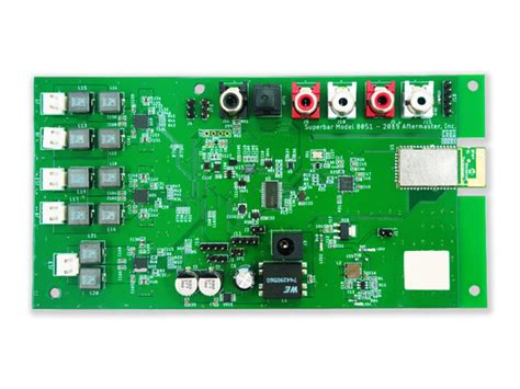
Streamlining the PCBA Assembly Process for Efficiency
Efficient PCB assembly requires a holistic approach that integrates design, material management, and process optimization. Central to this effort is the adoption of design for manufacturability (DFM) principles, which minimize errors and rework during PCBA production. By aligning layout designs with manufacturing capabilities—such as component spacing, pad sizes, and thermal management—engineers reduce bottlenecks and improve yield rates.
Automation plays a pivotal role in modern PCB assembly workflows. High-speed pick-and-place machines, automated optical inspection (AOI), and precision soldering systems ensure consistency while accelerating production cycles. For example, integrating surface-mount technology (SMT) with automated reflow ovens reduces manual intervention, enhancing throughput for high-volume PCBA orders.
Material logistics also impact efficiency. Just-in-time (JIT) inventory management for components, solder paste, and substrates prevents delays and reduces storage costs. Partnering with certified suppliers for critical materials like high-temperature laminates or lead-free solders ensures reliability without compromising turnaround times.
| Process Step | Manual Approach | Automated Approach |
|---|---|---|
| Component Placement | 20–30 minutes/board | 2–5 minutes/board |
| Soldering | Prone to inconsistencies | Consistent, repeatable results |
| Quality Inspection | Visual checks (error-prone) | AOI/X-ray (99.9% accuracy) |
Testing phases further streamline the PCBA process. In-circuit testing (ICT) and functional testing validate performance early, reducing post-production failures. Combining these with real-time data analytics allows manufacturers to identify trends, such as recurring solder joint defects, and refine processes proactively.
Ultimately, optimizing PCB assembly demands balancing speed, cost, and quality. By leveraging automation, DFM, and robust supply chains, teams achieve scalable, high-performance PCBA solutions that meet today’s demands for rapid, reliable electronics manufacturing.
Testing and Quality Assurance in PCB/PCBA Manufacturing
Effective testing and quality assurance (QA) are critical to ensuring the reliability and performance of PCB assembly (PCBA) products. Modern manufacturing processes employ a combination of automated and manual inspection techniques to identify defects early, minimize rework costs, and maintain compliance with industry standards. Automated optical inspection (AOI) and X-ray inspection are widely used to detect soldering flaws, component misalignment, or hidden issues like voids in ball grid arrays (BGAs). For high-density PCBA designs, in-circuit testing (ICT) validates electrical functionality by checking continuity, resistance, and signal integrity across critical nodes.
Environmental stress screening, such as thermal cycling and humidity testing, ensures boards withstand real-world operating conditions, while functional testing simulates end-use scenarios to verify system-level performance. To address evolving complexity, manufacturers increasingly integrate design-for-testability (DFT) principles during the PCB assembly phase, embedding test points and boundary scan capabilities for easier diagnostics.
Quality assurance extends beyond testing to encompass traceability and documentation. Advanced manufacturing execution systems (MES) track every stage of the PCBA process, linking defects to specific batches or components for rapid root-cause analysis. Compliance with standards like IPC-A-610 and ISO 9001 ensures consistency, while statistical process control (SPC) tools monitor production trends to preempt deviations.
Emerging technologies, such as AI-powered defect detection and 3D solder paste inspection (SPI), further enhance precision, reducing false positives and accelerating time-to-market. By prioritizing rigorous testing and QA protocols, manufacturers mitigate risks, improve yield rates, and deliver cost-effective, high-performance solutions that meet stringent industry demands.
Cost-Effective Design Practices for Scalable Production
Implementing cost-effective design practices in PCB assembly and PCBA development is critical for achieving scalable production without compromising quality. A foundational step involves optimizing component placement and layout to minimize material waste and reduce fabrication complexity. By standardizing component sizes and footprints, designers can lower procurement costs and streamline inventory management. Additionally, adhering to Design for Manufacturability (DFM) principles ensures compatibility with automated assembly processes, reducing the risk of rework or delays during PCBA production.
Leveraging panelization techniques—grouping multiple boards into a single panel—enhances manufacturing efficiency by maximizing machine utilization and minimizing handling time. However, designers must balance panel size with material yield to avoid excess waste. Using simulation tools to validate thermal performance and signal integrity early in the design phase helps prevent costly post-production modifications. For example, optimizing trace widths and spacing reduces the likelihood of signal interference, while strategic placement of heat-generating components mitigates thermal stress.
Material selection also plays a pivotal role in cost management. While high-performance substrates may be necessary for specialized applications, standard FR-4 laminates often suffice for general-purpose PCB assembly, offering a balance between cost and reliability. Bulk purchasing of common components and collaborating with suppliers for volume discounts further drives down per-unit expenses.
Finally, modular design approaches enable scalability by allowing reusable circuit blocks across product variants. This not only accelerates time-to-market but also simplifies upgrades and repairs. By integrating these strategies, manufacturers can achieve high-volume output with consistent quality, ensuring PCBA solutions remain competitive in dynamic markets.
Emerging Trends in PCB/PCBA Technology and Innovation
The PCB assembly landscape is evolving rapidly, driven by advancements in miniaturization, material science, and automation. One notable trend is the adoption of high-density interconnect (HDI) technology, which enables PCBA designs to accommodate more components in smaller footprints while maintaining signal integrity. This is particularly critical for applications like IoT devices and wearables, where space constraints demand ultra-compact layouts. Another emerging innovation is the integration of flexible and rigid-flex PCBs, which combine durability with bendability to support complex geometries in automotive and medical electronics.
Sustainability is also reshaping PCB assembly practices, with manufacturers prioritizing halogen-free substrates and recyclable materials to meet global environmental regulations. Additionally, the rise of additive manufacturing techniques, such as 3D-printed circuits, is reducing prototyping lead times and enabling rapid iteration for customized solutions.
Artificial intelligence (AI) and machine learning are increasingly embedded in PCBA production lines, optimizing defect detection and predictive maintenance. Automated optical inspection (AOI) systems now leverage AI algorithms to identify microscopic flaws in real time, significantly improving yield rates. Meanwhile, advancements in thermal management—like embedded heat sinks and advanced conformal coatings—are addressing challenges posed by high-power components in 5G and automotive systems.
The shift toward modular design in PCB assembly is another key development, allowing manufacturers to reuse standardized subassemblies across multiple products. This approach not only accelerates time-to-market but also reduces costs for scalable production. As the industry embraces these innovations, collaboration between designers and PCBA manufacturers remains essential to balance performance, reliability, and cost-effectiveness in next-generation electronic systems.
Conclusion
The evolution of PCB/PCBA design and manufacturing underscores the importance of integrating technical precision with strategic planning to achieve cost-effective, reliable, and high-performance electronic solutions. As the backbone of modern electronics, printed circuit board pcba systems demand meticulous attention to design fundamentals, material compatibility, and assembly workflows. By prioritizing layout optimization and adhering to design-for-manufacturability (DFM) principles, engineers can mitigate risks such as signal interference or thermal mismanagement, ensuring robust performance across applications.
Material selection plays a pivotal role in enhancing PCB reliability, particularly in harsh environments. Choices such as high-temperature laminates or low-loss substrates directly influence longevity and signal integrity. Similarly, streamlining the pcb assembly process through automated soldering, precision component placement, and rigorous quality assurance protocols reduces defects and accelerates time-to-market. Advanced testing methodologies, including automated optical inspection (AOI) and in-circuit testing (ICT), further safeguard against failures in PCBA units.
Emerging trends like high-density interconnect (HDI) technology, flexible PCBs, and IoT-driven miniaturization are reshaping industry standards, demanding agile adaptation from design teams. However, balancing innovation with cost-effective scalability remains critical—leveraging modular designs and standardized components can reduce overhead without compromising functionality. Ultimately, the synergy between forward-thinking design practices and disciplined manufacturing execution ensures that PCB/PCBA solutions meet both current demands and future challenges, solidifying their role as enablers of next-generation electronics.
Frequently Asked Questions
What is the difference between a PCB and a PCBA?
A PCB (Printed Circuit Board) is a bare board with conductive pathways etched onto it, while a PCBA (Printed Circuit Board Assembly) refers to a fully assembled board with components soldered onto the PCB. The pcb assembly process transforms a PCB into a functional electronic device.
How can I ensure high reliability in PCB design?
Focus on material selection, proper trace routing, and thermal management. Use high-quality substrates like FR-4 or specialized materials for extreme environments. Ensure compliance with industry standards such as IPC-A-610 for pcba manufacturing to minimize defects.
What are common challenges in PCBA assembly?
Issues like component misalignment, solder bridging, and thermal stress are common. Implementing automated optical inspection (AOI) and X-ray testing during pcb assembly helps identify defects early. Proper soldering profiles and component placement accuracy are critical.
How do I balance cost and performance in PCBA development?
Adopt design for manufacturability (DFM) principles to reduce waste and simplify assembly. Use standardized components where possible and optimize panelization to maximize material usage. For cost-effective pcba, prioritize critical performance areas while standardizing non-critical sections.
What testing methods are essential for quality assurance?
Functional testing, in-circuit testing (ICT), and environmental stress screening (ESS) validate pcba reliability. Automated testing tools ensure consistency, while boundary scan testing checks complex integrated circuits.
How do emerging technologies impact PCB/PCBA design?
Trends like high-density interconnects (HDI), flexible PCBs, and IoT-optimized designs demand advanced pcb assembly techniques. Innovations in materials, such as low-loss dielectrics, enhance signal integrity for high-frequency applications.
Can I reuse existing PCB designs for new projects?
Yes, modular design strategies allow repurposing proven circuit blocks. However, always validate compatibility with new pcba requirements, such as power demands or thermal constraints, to avoid performance issues.
Ready to Optimize Your PCB Assembly Process?
For expert guidance on pcb assembly and high-performance pcba solutions, please click here to explore tailored services that align with your project needs.