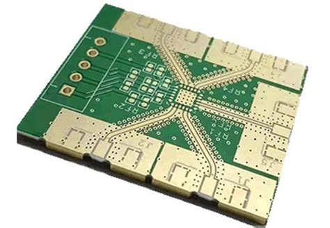
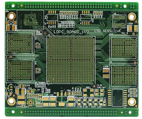
Pcb prototype fabrication
Understanding The Basics Of PCB Prototype Fabrication
Printed Circuit Board (PCB) prototype fabrication is a critical process in the development of electronic devices, serving as the foundation upon which electronic circuits are built. Understanding the basics of this process is essential for engineers, designers, and anyone involved in the creation of electronic products. The journey begins with the design phase, where the schematic diagram of the circuit is translated into a layout that can be physically realized on a PCB. This layout includes the placement of components and the routing of electrical connections between them.
Once the design is finalized, the next step involves selecting the appropriate materials.
Typically, PCBs are made from a substrate material, such as fiberglass-reinforced epoxy laminate, which provides mechanical support and electrical insulation. The most common type of substrate is FR-4, known for its durability and thermal resistance. On top of the substrate, a thin layer of conductive material, usually copper, is applied. This copper layer is where the electrical pathways, or traces, will be etched.
The fabrication process begins with the transfer of the PCB design onto the copper-clad substrate.
This is often achieved through a method called photolithography, where a photoresist material is applied to the copper surface. The photoresist is then exposed to ultraviolet light through a mask that represents the PCB layout. The areas exposed to light harden, while the unexposed areas remain soft and can be washed away, leaving behind a pattern of the circuit design.
Following the photolithography process, the next step is etching.
During etching, the board is submerged in a chemical solution that removes the unprotected copper, leaving only the desired circuit traces. This step is crucial, as it defines the electrical pathways that will connect the various components on the PCB. After etching, the remaining photoresist is stripped away, revealing the final copper traces.
To ensure the PCB can accommodate electronic components, holes must be drilled at precise locations.
These holes, known as vias, allow for electrical connections between different layers of the PCB or for mounting components. Advanced PCBs may have multiple layers, requiring careful alignment and drilling to maintain connectivity across layers.
Once drilling is complete, the PCB undergoes a process called plating, where the holes are coated with a thin layer of conductive material, typically copper, to ensure electrical continuity.
This is followed by the application of a solder mask, a protective layer that insulates the copper traces and prevents solder bridges during component assembly. The solder mask also gives the PCB its characteristic green color, although other colors are available.
The final step in PCB prototype fabrication is the application of a silkscreen layer. This layer contains printed information, such as component labels and reference designators, which aid in the assembly and troubleshooting of the PCB. The silkscreen is typically applied using a screen-printing process.
In conclusion, PCB prototype fabrication is a meticulous process that transforms a circuit design into a functional physical entity. Each step, from design transfer to silkscreen application, plays a vital role in ensuring the reliability and performance of the final product. By understanding these basics, one can appreciate the complexity and precision required to create the electronic devices that power our modern world.
Top Tools And Software For PCB Prototype Design
Printed Circuit Board (PCB) prototype fabrication is a critical phase in the development of electronic devices, serving as a bridge between conceptual design and mass production. To ensure the success of this phase, engineers and designers rely on a variety of tools and software that streamline the design process, enhance accuracy, and reduce the likelihood of errors. Among the top tools and software for PCB prototype design, several stand out due to their comprehensive features and user-friendly interfaces.
One of the most widely used tools in PCB prototype design is Altium Designer.
This software is renowned for its robust set of features that cater to both novice and experienced designers. Altium Designer offers a unified design environment, which means that all aspects of PCB design, from schematic capture to layout and routing, are integrated into a single platform. This integration facilitates seamless transitions between different stages of the design process, thereby improving efficiency and reducing the risk of inconsistencies. Additionally, Altium Designer supports advanced features such as 3D visualization, which allows designers to inspect their designs in a three-dimensional space, ensuring that all components fit together as intended.
Transitioning to another essential tool, Eagle PCB, developed by Autodesk, is also highly regarded in the industry.
Eagle PCB is particularly popular among hobbyists and small-scale developers due to its affordability and ease of use. Despite its relatively lower cost, Eagle PCB does not compromise on functionality. It provides a comprehensive suite of tools for schematic capture, board layout, and auto-routing. Moreover, Eagle PCB’s extensive library of components and its active user community make it easier for designers to find the parts they need and get support when they encounter challenges.
In addition to these, KiCad is an open-source alternative that has gained significant traction in recent years.
KiCad’s appeal lies in its cost-free nature and its powerful capabilities that rival those of commercial software. It includes tools for schematic capture, PCB layout, and even a 3D viewer. KiCad’s open-source nature means that it is continuously being improved by a global community of developers, ensuring that it stays up-to-date with the latest advancements in PCB design technology. Furthermore, KiCad’s flexibility allows users to customize the software to suit their specific needs, making it a versatile choice for a wide range of projects.
Another noteworthy mention is OrCAD, a professional-grade tool that is widely used in the industry for complex PCB designs.
OrCAD excels in handling large-scale projects with intricate requirements. Its powerful simulation capabilities allow designers to test their circuits under various conditions before committing to a physical prototype. This predictive analysis helps in identifying potential issues early in the design process, thereby saving time and resources.
Finally, it is important to highlight the role of simulation software such as SPICE (Simulation Program with Integrated Circuit Emphasis).
SPICE is not a PCB design tool per se, but it is indispensable for verifying the functionality of electronic circuits. By simulating the behavior of circuits, SPICE helps designers ensure that their designs will perform as expected in real-world conditions.
In conclusion, the selection of tools and software for PCB prototype design is crucial for the successful development of electronic devices. Altium Designer, Eagle PCB, KiCad, OrCAD, and SPICE each offer unique advantages that cater to different aspects of the design process. By leveraging these tools, designers can enhance their productivity, improve the accuracy of their designs, and ultimately bring innovative electronic products to market more efficiently.
Common Challenges In PCB Prototype Fabrication And How To Overcome Them
PCB prototype fabrication is a critical phase in the development of electronic devices, serving as a bridge between design and mass production. However, this process is fraught with challenges that can impede progress and affect the final product’s quality. Understanding these common challenges and how to overcome them is essential for engineers and designers aiming to achieve optimal results.
One of the primary challenges in PCB prototype fabrication is ensuring design accuracy.
Even minor errors in the design phase can lead to significant issues during fabrication. To mitigate this, it is crucial to conduct thorough design reviews and simulations. Utilizing advanced design software that offers real-time error checking can help identify potential problems early. Additionally, collaborating closely with the fabrication team during the design phase can provide valuable insights and preemptively address any manufacturability concerns.
Another significant challenge is material selection.
The choice of materials impacts not only the performance but also the durability and cost of the PCB. Engineers must consider factors such as thermal conductivity, electrical insulation, and mechanical strength. To overcome this, it is advisable to consult with material experts and conduct extensive testing of different materials under various conditions. This approach ensures that the selected materials meet the specific requirements of the application, thereby enhancing the overall reliability of the PCB.
The complexity of modern PCBs, with their multi-layered structures and high component density, presents another hurdle.
Managing signal integrity and minimizing electromagnetic interference (EMI) are critical in such designs. To address these issues, designers should employ best practices such as proper layer stacking, controlled impedance routing, and the use of ground planes. Additionally, simulation tools can be used to predict and mitigate potential signal integrity and EMI problems before fabrication.
Manufacturing tolerances also pose a challenge in PCB prototype fabrication.
Variations in etching, drilling, and plating processes can lead to discrepancies between the designed and fabricated PCBs. To minimize these variations, it is essential to work with reputable fabrication partners who adhere to stringent quality control standards. Regular communication with the fabrication team can also help in understanding their capabilities and limitations, allowing for design adjustments that accommodate manufacturing tolerances.
Time constraints are another common issue in PCB prototype fabrication.
The pressure to meet tight deadlines can lead to rushed processes and oversight of critical details. To manage this, it is beneficial to adopt a structured project management approach, with clear timelines and milestones. Prioritizing tasks and maintaining open lines of communication among all stakeholders can ensure that the project stays on track without compromising quality.
Cost management is a perennial challenge in PCB prototype fabrication.
Balancing the need for high-quality prototypes with budget constraints requires careful planning and resource allocation. One effective strategy is to adopt a phased approach, starting with simpler, lower-cost prototypes to validate basic design concepts before moving on to more complex and expensive iterations. Additionally, leveraging economies of scale by consolidating orders or partnering with other projects can help reduce costs.
In conclusion, PCB prototype fabrication is a complex process that involves navigating various challenges, from design accuracy and material selection to managing manufacturing tolerances and time constraints. By adopting a proactive approach that includes thorough planning, collaboration, and the use of advanced tools and techniques, these challenges can be effectively managed. This not only ensures the successful fabrication of high-quality PCBs but also paves the way for a smoother transition to mass production.
Innovative Techniques In Modern PCB Prototype Fabrication
In the realm of electronics, the fabrication of printed circuit board (PCB) prototypes has undergone significant advancements, driven by the need for more efficient, reliable, and compact designs. Modern PCB prototype fabrication techniques have evolved to meet the increasing demands of various industries, including telecommunications, automotive, and consumer electronics. These innovative methods not only enhance the performance and functionality of electronic devices but also streamline the manufacturing process, reducing time and costs.
One of the most notable advancements in PCB prototype fabrication is the adoption of surface mount technology (SMT).
Unlike traditional through-hole technology, SMT allows components to be mounted directly onto the surface of the PCB, thereby enabling higher component density and more complex circuit designs. This technique has revolutionized the industry by allowing for smaller, lighter, and more efficient electronic devices. Moreover, SMT facilitates automated assembly processes, which significantly reduce production time and improve consistency in manufacturing.
In addition to SMT, the use of advanced materials has also played a crucial role in modern PCB prototype fabrication.
High-frequency laminates, for instance, are now commonly used in the production of PCBs for high-speed and high-frequency applications. These materials offer superior electrical performance, reduced signal loss, and improved thermal management, making them ideal for applications such as 5G telecommunications and advanced radar systems. Furthermore, the development of flexible and rigid-flex PCBs has opened new possibilities for innovative product designs, particularly in wearable technology and medical devices.
Another significant innovation in PCB prototype fabrication is the implementation of additive manufacturing techniques, commonly known as 3D printing.
This approach allows for the creation of complex PCB structures with intricate geometries that would be challenging or impossible to achieve using traditional subtractive methods. By depositing conductive and insulating materials layer by layer, 3D printing enables rapid prototyping and customization of PCBs, thereby accelerating the design and testing phases of product development. Additionally, this technique minimizes material waste and reduces the environmental impact of PCB manufacturing.
The integration of advanced computer-aided design (CAD) software and simulation tools has further enhanced the PCB prototype fabrication process.
These tools enable engineers to design, analyze, and optimize PCB layouts with greater precision and efficiency. By simulating the electrical, thermal, and mechanical performance of a PCB before physical fabrication, potential issues can be identified and addressed early in the design process. This not only improves the overall quality and reliability of the final product but also reduces the likelihood of costly design revisions and rework.
Moreover, the advent of automated optical inspection (AOI) and X-ray inspection technologies has significantly improved the quality control and testing of PCB prototypes. AOI systems use high-resolution cameras and sophisticated algorithms to detect defects such as solder joint issues, component misalignment, and surface contamination. X-ray inspection, on the other hand, allows for the examination of hidden features and internal structures, ensuring the integrity of multi-layer PCBs and identifying potential defects that are not visible to the naked eye. These inspection techniques enhance the reliability and performance of PCB prototypes, ultimately leading to higher-quality end products.
In conclusion, the field of PCB prototype fabrication has seen remarkable advancements in recent years, driven by the adoption of innovative techniques such as surface mount technology, advanced materials, additive manufacturing, and sophisticated design and inspection tools. These developments have not only improved the performance and functionality of electronic devices but also streamlined the manufacturing process, making it more efficient and cost-effective. As technology continues to evolve, it is likely that we will witness further innovations in PCB prototype fabrication, paving the way for even more advanced and reliable electronic products.


