Pcb prototype fabrication service
Benefits Of Using A PCB Prototype Fabrication Service
The utilization of a PCB prototype fabrication service offers numerous advantages that can significantly enhance the development process of electronic devices. One of the primary benefits is the ability to test and validate designs before committing to full-scale production.
By creating a prototype, engineers can identify and rectify any design flaws or functional issues early in the development cycle.
This preemptive troubleshooting not only saves time but also reduces the costs associated with potential rework or redesigns in later stages.
Moreover, PCB prototype fabrication services provide access to advanced manufacturing technologies and expertise that may not be readily available in-house.
These services often employ state-of-the-art equipment and skilled technicians who are adept at handling complex designs and intricate circuitry. Consequently, leveraging such specialized resources ensures that the prototypes are produced with high precision and quality, which is crucial for the performance and reliability of the final product.
In addition to technical advantages, using a PCB prototype fabrication service can also streamline the project timeline.
These services are designed to expedite the prototyping process, offering quick turnaround times that can accelerate the overall development schedule. This rapid prototyping capability is particularly beneficial in industries where time-to-market is a critical factor, such as consumer electronics, automotive, and telecommunications. By reducing the time required to move from concept to prototype, companies can gain a competitive edge and respond more swiftly to market demands.
Furthermore, PCB prototype fabrication services often provide comprehensive support throughout the prototyping phase.
This support can include design consultation, material selection, and even assistance with regulatory compliance. Such holistic support ensures that the prototype not only meets the technical specifications but also adheres to industry standards and regulations. This is especially important in sectors where compliance with stringent safety and performance standards is mandatory.
Another significant benefit is the ability to experiment with different design iterations without incurring substantial costs.
Prototyping allows for iterative testing and refinement, enabling designers to explore various configurations and optimize the design for performance, manufacturability, and cost-effectiveness. This iterative approach fosters innovation and can lead to the development of more efficient and effective electronic solutions.
Additionally, PCB prototype fabrication services can facilitate better communication and collaboration among project stakeholders.
By providing tangible prototypes, engineers, designers, and clients can engage in more meaningful discussions and feedback sessions. This collaborative environment helps ensure that the final product aligns with the intended design and functionality, ultimately leading to higher customer satisfaction.
Cost efficiency is another notable advantage of using a PCB prototype fabrication service.
While the initial investment in prototyping may seem significant, it is often more economical in the long run. Early detection and correction of design issues can prevent costly mistakes and production delays. Moreover, many fabrication services offer scalable solutions, allowing companies to adjust their prototyping needs based on project requirements and budget constraints.
In conclusion, the benefits of using a PCB prototype fabrication service are multifaceted, encompassing technical precision, expedited timelines, comprehensive support, iterative design capabilities, enhanced collaboration, and cost efficiency. By leveraging these services, companies can improve the quality and reliability of their electronic products, reduce development risks, and achieve faster time-to-market. As the demand for sophisticated electronic devices continues to grow, the role of PCB prototype fabrication services in the development process becomes increasingly indispensable.
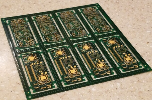
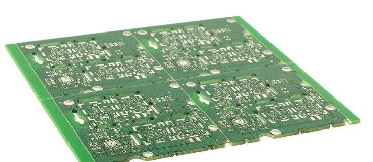
Key Steps In The PCB Prototype Fabrication Process
The process of PCB prototype fabrication is a critical phase in the development of electronic devices, serving as a bridge between the initial design and mass production. Understanding the key steps involved in this process is essential for ensuring the functionality and reliability of the final product.
The journey begins with the design phase, where engineers use specialized software to create a detailed schematic of the circuit. This schematic is then translated into a layout, which specifies the exact placement of components and the routing of electrical connections on the board.
Once the design is finalized, the next step is to generate the Gerber files, which are the industry-standard format for PCB manufacturing.
These files contain all the necessary information about the board’s layers, including the copper traces, solder mask, and silkscreen. The Gerber files are then sent to the fabrication facility, where the actual production begins.
The fabrication process starts with the selection of the base material, typically a fiberglass-reinforced epoxy laminate known as FR4.
This material is chosen for its excellent electrical insulation properties and mechanical strength. The copper-clad laminate is then cleaned to remove any contaminants that could affect the adhesion of the photoresist, a light-sensitive material that is applied to the surface of the board.
Following the application of the photoresist, the board is exposed to ultraviolet light through a photomask, which contains the pattern of the circuit.
The areas of the photoresist exposed to the light harden, while the unexposed areas remain soft and are subsequently washed away, revealing the underlying copper. The next step is the etching process, where a chemical solution is used to remove the unwanted copper, leaving behind the desired circuit pattern.
After etching, the board undergoes a series of cleaning and inspection steps to ensure that the copper traces are free of defects.
The next phase involves the application of the solder mask, which is a protective layer that prevents solder bridges from forming between closely spaced components during assembly. The solder mask is applied as a liquid and then cured using ultraviolet light.
The application of the silkscreen follows, which involves printing component labels and other important information on the board.
This step is crucial for the assembly process, as it helps technicians identify the correct placement of components. Once the silkscreen is applied, the board is subjected to a final inspection to ensure that all layers are correctly aligned and free of defects.
The final step in the PCB prototype fabrication process is the drilling of holes for through-hole components and vias, which are used to connect different layers of the board. This is typically done using computer-controlled drilling machines that ensure precise placement and sizing of the holes. After drilling, the holes are plated with copper to establish electrical connections between the layers.
In conclusion, the PCB prototype fabrication process involves a series of meticulously executed steps, each of which plays a crucial role in ensuring the functionality and reliability of the final product. From the initial design and generation of Gerber files to the application of solder mask and silkscreen, each phase requires careful attention to detail and adherence to industry standards. By understanding these key steps, engineers and manufacturers can work together to produce high-quality PCB prototypes that meet the rigorous demands of modern electronic devices.
How To Choose The Right PCB Prototype Fabrication Service
Selecting the right PCB prototype fabrication service is a critical step in the development of any electronic product. The process involves several key considerations that can significantly impact the quality, cost, and timeline of your project. To make an informed decision, it is essential to evaluate various factors that contribute to the overall effectiveness of the service provider.
First and foremost, the technical capabilities of the fabrication service should be thoroughly assessed.
This includes examining the range of materials they can work with, the precision of their manufacturing processes, and their ability to handle complex designs. A service provider with advanced technological capabilities will be better equipped to meet the specific requirements of your project, ensuring that the final product meets the highest standards of quality and performance.
In addition to technical capabilities, the experience and expertise of the service provider play a crucial role.
Companies with a proven track record in PCB prototype fabrication are more likely to deliver reliable and high-quality results. It is advisable to review their portfolio and seek feedback from previous clients to gauge their level of expertise and reliability. An experienced provider will also be more adept at identifying potential issues early in the process, thereby minimizing the risk of costly errors and delays.
Another important consideration is the turnaround time offered by the fabrication service.
In the fast-paced world of electronics, time-to-market is often a critical factor. A service provider that can deliver prototypes quickly without compromising on quality can give you a significant competitive advantage. It is important to inquire about their lead times and ensure that they have the capacity to meet your project deadlines.
Cost is, of course, a major factor in the decision-making process.
While it may be tempting to opt for the lowest-priced service, it is important to consider the overall value offered. A low-cost provider may cut corners, resulting in subpar quality and potential issues down the line. It is essential to strike a balance between cost and quality, ensuring that you receive a high-quality product at a reasonable price. Requesting detailed quotes and comparing them can help you make a more informed decision.
Communication and customer support are also vital aspects to consider.
A service provider that maintains clear and open lines of communication can greatly enhance the overall experience. They should be responsive to your inquiries, provide regular updates on the progress of your project, and be willing to address any concerns that may arise. Effective communication can help prevent misunderstandings and ensure that the final product aligns with your expectations.
Furthermore, it is important to consider the range of services offered by the fabrication provider.
Some companies offer end-to-end solutions, including design, fabrication, assembly, and testing. Opting for a provider that offers a comprehensive suite of services can simplify the process and reduce the need for multiple vendors. This can lead to better coordination, faster turnaround times, and potentially lower costs.
Lastly, it is advisable to consider the geographical location of the service provider.
While advancements in technology have made it easier to work with providers from around the world, there can still be advantages to choosing a local provider. These may include easier communication, faster shipping times, and the ability to visit the facility if needed.
In conclusion, choosing the right PCB prototype fabrication service requires careful consideration of several factors, including technical capabilities, experience, turnaround time, cost, communication, range of services, and geographical location. By thoroughly evaluating these aspects, you can select a service provider that will deliver high-quality prototypes, helping to ensure the success of your electronic product development.
Common Challenges In PCB Prototype Fabrication And How To Overcome Them
PCB prototype fabrication is a critical phase in the development of electronic devices, serving as a bridge between the conceptual design and mass production. However, this process is fraught with numerous challenges that can impede progress and affect the final product’s quality. Understanding these common challenges and knowing how to overcome them is essential for ensuring a successful outcome.
One of the primary challenges in PCB prototype fabrication is the complexity of the design.
As electronic devices become more sophisticated, the corresponding PCB designs also grow in complexity. This complexity can lead to issues such as signal interference, thermal management problems, and difficulties in routing traces. To mitigate these issues, it is crucial to employ advanced design software that can handle intricate layouts and provide simulation capabilities. Additionally, involving experienced engineers in the design phase can help identify potential problems early on and devise effective solutions.
Another significant challenge is the selection of materials.
The choice of substrate, copper thickness, and solder mask can greatly influence the performance and reliability of the PCB. Inappropriate material selection can result in issues such as delamination, warping, and poor thermal conductivity. To address this, it is important to thoroughly understand the requirements of the specific application and select materials that meet those needs. Consulting with material experts and conducting thorough testing can also help ensure that the chosen materials will perform as expected under various conditions.
Manufacturing tolerances present another hurdle in PCB prototype fabrication.
Even minor deviations in dimensions can lead to misalignment, poor connectivity, and ultimately, a non-functional prototype. To overcome this, it is essential to work with reputable fabrication houses that adhere to strict quality control standards. Employing precision manufacturing techniques and conducting rigorous inspections at various stages of the fabrication process can also help maintain tight tolerances and ensure the prototype meets the desired specifications.
Time constraints are often a pressing issue in PCB prototype fabrication.
The need to quickly iterate and test designs can put pressure on the fabrication process, leading to rushed decisions and potential errors. To manage this, it is beneficial to adopt a systematic approach to prototyping that includes clear timelines, milestones, and contingency plans. Utilizing rapid prototyping services that offer quick turnaround times without compromising on quality can also be advantageous.
Cost considerations cannot be overlooked when discussing challenges in PCB prototype fabrication.
The expenses associated with materials, manufacturing, and testing can quickly add up, especially when multiple iterations are required. To keep costs under control, it is important to conduct a thorough cost-benefit analysis during the design phase. Exploring different fabrication options, such as using standard components and processes, can also help reduce expenses. Additionally, collaborating with suppliers to negotiate better rates and leveraging economies of scale can further drive down costs.
In conclusion, while PCB prototype fabrication presents several challenges, understanding these obstacles and implementing strategic measures can significantly enhance the likelihood of success. By addressing design complexity, selecting appropriate materials, maintaining manufacturing tolerances, managing time constraints, and controlling costs, it is possible to navigate the intricacies of PCB prototype fabrication effectively. This approach not only ensures the development of high-quality prototypes but also paves the way for a smoother transition to mass production, ultimately contributing to the creation of reliable and efficient electronic devices.


