Pcb prototype production
Essential Steps in PCB Prototype Production
Printed Circuit Board (PCB) prototype production is a critical phase in the development of electronic devices, serving as a preliminary model to test and validate the design before mass production. The process involves several essential steps, each contributing to the overall functionality and reliability of the final product. Understanding these steps is crucial for engineers and designers aiming to create efficient and effective electronic circuits.
The initial step in PCB prototype production is the design phase, where engineers use specialized software to create a schematic diagram of the circuit.
This diagram serves as a blueprint, detailing the electrical connections and components required for the PCB. During this phase, it is imperative to consider factors such as component placement, signal integrity, and thermal management to ensure optimal performance. Once the schematic is complete, it is converted into a layout design, which specifies the physical arrangement of components and the routing of electrical traces on the board.
Following the design phase, the next step is to generate the Gerber files, which are the standard format for PCB manufacturing.
These files contain detailed information about each layer of the PCB, including the copper traces, solder mask, and silkscreen. It is essential to review these files meticulously to identify and correct any potential errors before proceeding to fabrication. This step is crucial as any mistake at this stage can lead to costly revisions and delays in the production process.
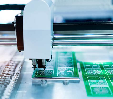
Once the Gerber files are finalized, the fabrication process begins.
This involves the creation of the PCB substrate, typically made from a fiberglass-reinforced epoxy laminate material. The substrate is coated with a layer of copper, which is then etched away to form the desired circuit pattern. This etching process is highly precise, ensuring that the copper traces are accurately formed according to the design specifications. After etching, the board undergoes a series of cleaning and inspection steps to remove any residual chemicals and ensure the integrity of the copper traces.
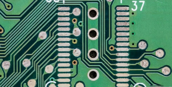
Subsequently, the PCB is drilled to create holes for component leads and vias, which are used to connect different layers of the board.
The drilling process must be executed with high precision to avoid damaging the board and ensure proper alignment of the holes. Following drilling, the board is plated with a thin layer of copper to establish electrical connections between the layers. This step is followed by the application of a solder mask, which protects the copper traces from oxidation and prevents solder bridges during component assembly.
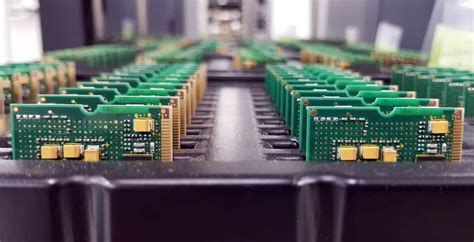
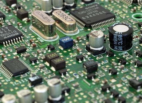
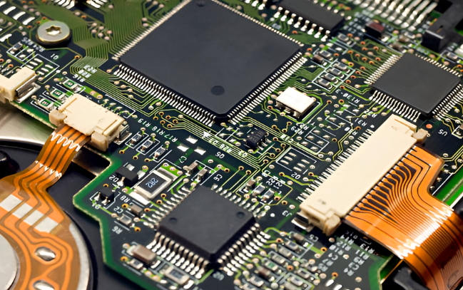
The final step in PCB prototype production is the assembly process, where components are mounted onto the board.
This can be done using either surface-mount technology (SMT) or through-hole technology, depending on the design requirements. During assembly, it is crucial to ensure that components are placed accurately and soldered correctly to avoid any functional issues. Once assembly is complete, the prototype undergoes rigorous testing to verify its performance and identify any potential defects.
In conclusion, PCB prototype production is a multifaceted process that requires careful planning and execution at each stage. From the initial design and generation of Gerber files to the fabrication, drilling, and assembly, each step plays a vital role in ensuring the success of the final product. By adhering to these essential steps and maintaining a high level of precision and attention to detail, engineers and designers can create reliable and efficient PCB prototypes that pave the way for successful mass production.
Common Challenges in PCB Prototype Manufacturing
PCB prototype manufacturing is a critical phase in the development of electronic devices, serving as a bridge between design and mass production. However, this process is fraught with numerous challenges that can impede progress and affect the final product’s quality. One of the most common challenges is ensuring the accuracy of the design files. Any discrepancies between the design and the actual prototype can lead to functional failures, necessitating costly and time-consuming revisions. Therefore, meticulous attention to detail during the design phase is paramount.
Another significant challenge is the selection of materials.
The choice of substrate, copper thickness, and solder mask can greatly influence the performance and durability of the PCB. For instance, using a substrate that cannot withstand high temperatures may result in warping or delamination during soldering. Consequently, engineers must carefully consider the operational environment and electrical requirements when selecting materials.
Transitioning from design to physical production introduces the challenge of manufacturing tolerances.
Even minor deviations in etching, drilling, or layer alignment can compromise the PCB’s functionality. To mitigate this, manufacturers often employ advanced fabrication techniques and rigorous quality control measures. However, these methods can increase production costs and extend lead times, posing a dilemma for projects with tight budgets and schedules.
Furthermore, the miniaturization of electronic components has exacerbated the complexity of PCB prototypes.
As devices become smaller and more powerful, the need for high-density interconnects (HDI) and multi-layer PCBs has grown. This trend necessitates precise manufacturing processes and advanced equipment, which can be prohibitively expensive for smaller firms. Additionally, the increased complexity raises the likelihood of defects, making thorough testing and inspection indispensable.
Thermal management is another critical issue in PCB prototype manufacturing.
As electronic components generate heat during operation, inadequate thermal management can lead to overheating and failure. Effective thermal management strategies, such as the use of thermal vias, heat sinks, and appropriate layout designs, are essential to ensure the reliability and longevity of the PCB. However, implementing these strategies can be challenging, particularly in compact designs where space is limited.
Moreover, the rapid pace of technological advancements presents a continuous challenge.
As new materials, components, and manufacturing techniques emerge, staying abreast of these developments is crucial for maintaining competitiveness. This requires ongoing investment in research and development, as well as continuous training for engineers and technicians.
Supply chain issues also pose significant challenges in PCB prototype manufacturing.
Sourcing high-quality components and materials can be difficult, especially in times of global shortages or geopolitical tensions. Delays in the supply chain can disrupt production schedules and increase costs. To mitigate these risks, manufacturers often establish relationships with multiple suppliers and maintain buffer stocks, although these measures can add to the overall expense.
Finally, regulatory compliance is a critical consideration in PCB prototype manufacturing.
Different regions have varying standards and regulations regarding materials, safety, and environmental impact. Ensuring compliance with these regulations is essential to avoid legal repercussions and ensure market access. This often involves extensive documentation and testing, which can be both time-consuming and costly.
In conclusion, PCB prototype manufacturing is a complex and multifaceted process that involves numerous challenges. From design accuracy and material selection to manufacturing tolerances and thermal management, each step requires careful consideration and meticulous execution. By understanding and addressing these challenges, manufacturers can improve the quality and reliability of their prototypes, paving the way for successful mass production.

Innovative Techniques for Rapid PCB Prototyping
In the realm of electronics, the demand for rapid and efficient PCB (Printed Circuit Board) prototyping has never been more critical. As technology advances at an unprecedented pace, the need for innovative techniques to expedite the prototyping process becomes paramount. One of the most significant advancements in this field is the adoption of additive manufacturing, commonly known as 3D printing. This technique allows for the creation of complex PCB designs with a high degree of precision and minimal material waste. By layering conductive and insulating materials, 3D printing can produce functional prototypes in a fraction of the time required by traditional methods.
Transitioning from traditional subtractive methods, such as etching, to additive manufacturing offers several advantages.
Notably, it reduces the lead time and cost associated with prototyping. Traditional methods often involve multiple steps, including designing, printing masks, etching, and drilling, each of which can introduce delays and errors. In contrast, 3D printing streamlines the process by integrating these steps into a single, automated workflow. This not only accelerates production but also enhances the accuracy and repeatability of the prototypes.
Another innovative technique gaining traction is the use of flexible PCBs.
Unlike rigid boards, flexible PCBs can be bent and folded to fit into compact and irregularly shaped spaces. This flexibility is particularly advantageous in the development of wearable technology and compact electronic devices. The production of flexible PCBs involves the use of flexible substrates, such as polyimide, which can withstand high temperatures and mechanical stress. By leveraging these materials, engineers can create prototypes that are not only functional but also adaptable to various form factors.
Moreover, the integration of advanced simulation software has revolutionized the PCB prototyping process.
These tools enable engineers to model and analyze the electrical and thermal performance of their designs before physical production. By simulating different scenarios, potential issues can be identified and addressed early in the design phase, thereby reducing the likelihood of costly revisions. This predictive capability is particularly beneficial in the development of high-frequency and high-power applications, where even minor design flaws can have significant implications.
In addition to these techniques, the adoption of automated assembly processes has further enhanced the efficiency of PCB prototyping.
Automated pick-and-place machines, for instance, can accurately position and solder components onto the board, significantly reducing the time and labor required for manual assembly. This automation not only speeds up production but also improves the consistency and reliability of the prototypes. Furthermore, advancements in surface-mount technology (SMT) have enabled the placement of smaller and more densely packed components, thereby increasing the functionality of the prototypes without expanding their footprint.
Lastly, the use of advanced materials, such as high-frequency laminates and thermal management substrates, has expanded the capabilities of PCB prototypes.
These materials offer superior electrical and thermal properties, making them ideal for demanding applications such as telecommunications and aerospace. By incorporating these materials into their designs, engineers can create prototypes that meet stringent performance requirements while maintaining manufacturability.
In conclusion, the landscape of PCB prototyping is continually evolving, driven by the need for faster, more efficient, and more versatile production methods. The adoption of 3D printing, flexible substrates, advanced simulation software, automated assembly processes, and cutting-edge materials has collectively transformed the prototyping process. These innovative techniques not only accelerate the development cycle but also enhance the quality and functionality of the prototypes, thereby enabling engineers to bring their designs to market with greater confidence and speed.
Cost-Effective Strategies for PCB Prototype Development
In the realm of electronics, the development of printed circuit board (PCB) prototypes is a critical step in the design and manufacturing process. Ensuring that these prototypes are both functional and cost-effective is paramount for engineers and companies alike. To achieve this, several strategies can be employed, each contributing to the overall efficiency and affordability of the prototype development process.
One of the foremost strategies is to adopt a design-for-manufacturability (DFM) approach.
By considering manufacturing constraints during the design phase, engineers can minimize potential issues that may arise during production. This proactive approach not only reduces the likelihood of costly revisions but also streamlines the manufacturing process, leading to significant cost savings. For instance, standardizing component sizes and using commonly available materials can simplify assembly and reduce material costs.
Another effective strategy is to leverage advanced simulation and modeling tools.
These tools allow engineers to virtually test and validate their designs before committing to physical prototypes. By identifying and addressing potential issues early in the design process, companies can avoid the expenses associated with multiple iterations of physical prototypes. Additionally, simulation tools can optimize the layout and performance of the PCB, further enhancing its cost-effectiveness.
Furthermore, selecting the right manufacturing partner is crucial for cost-effective PCB prototype development.
Partnering with a manufacturer that offers competitive pricing, reliable quality, and efficient turnaround times can significantly impact the overall cost. It is advisable to conduct thorough research and seek recommendations to identify a manufacturer that aligns with the specific needs and budget constraints of the project. Additionally, some manufacturers offer value-added services such as design reviews and technical support, which can further enhance the cost-effectiveness of the prototype development process.
In addition to choosing the right manufacturing partner, it is essential to consider the economies of scale.
Ordering PCBs in larger quantities can often result in lower per-unit costs due to bulk pricing discounts. While this may not always be feasible for initial prototypes, it is a strategy worth considering as the project progresses towards production. Balancing the need for prototype iterations with the benefits of bulk ordering can lead to substantial cost savings in the long run.
Moreover, adopting a modular design approach can also contribute to cost-effective PCB prototype development.
By designing PCBs in modular sections, engineers can test and validate individual modules before integrating them into the final design. This approach not only reduces the risk of costly errors but also allows for easier troubleshooting and modifications. Additionally, modular designs can be reused across different projects, further enhancing their cost-effectiveness.
Lastly, effective communication and collaboration among all stakeholders are vital for ensuring cost-effective PCB prototype development.
Clear and consistent communication between designers, engineers, and manufacturers can prevent misunderstandings and ensure that everyone is aligned with the project goals and requirements. Regular meetings and updates can help identify potential issues early and facilitate timely resolutions, ultimately reducing the risk of costly delays and rework.
In conclusion, achieving cost-effective PCB prototype development requires a multifaceted approach that encompasses design considerations, advanced tools, strategic partnerships, economies of scale, modular design, and effective communication. By implementing these strategies, companies can not only reduce the overall cost of prototype development but also enhance the quality and reliability of their final products.