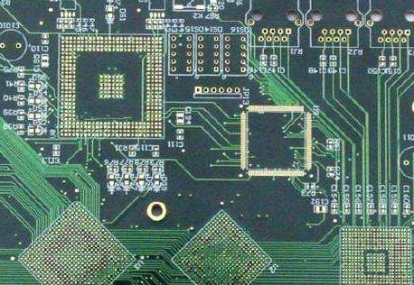
pcb quality control

1. What are the quality problems of PCB? How to improve and enhance them?
(1) Poor solderability
Solderability is also one of the more serious problems, especially the batch problem. The possible causes are board surface pollution, oxidation, black nickel, abnormal nickel thickness, solder mask SCUM (shadow), long storage time, moisture absorption, solder mask on PAD, too thick (repair).
Poor pollution and moisture absorption are relatively easy to solve, while other problems are more troublesome and cannot be found through incoming material inspection. At this time, it is necessary to pay attention to the process capability and quality control plan of the PCB board factory.
For example, for black nickel, it is necessary to see whether the PCB factory outsources the gold processing, whether the frequency of analyzing its own gold wire solution is sufficient, whether the concentration is stable, whether regular gold stripping tests and phosphorus content tests are set up for detection, and whether the internal solderability test is well executed. If all of these can be done well, the possibility of batch problems is very small.
As for the poor PAD and repair on solder mask, it is necessary to understand the standards set by the PCB supplier for inspection and maintenance, whether the inspectors and maintenance personnel have a good assessment and employment system, and clearly define that the dense pad areas cannot be repaired (such as BGA and OFP).

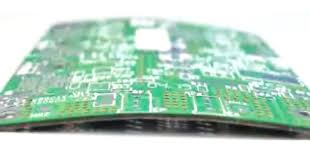
(2) Board bending and warping
The reasons that may cause board bending and warping include: supplier material selection problems, abnormal production process, poor rework control, improper transportation or storage, insufficient design of broken holes, and large differences in copper area of each layer.
The last two design problems need to be avoided through design review in the early stage. At the same time, the PCB factory can be required to simulate the mounting conditions I for testing to avoid the bad board bending after the furnace.
For some boards, it can be required to pack the wood pulp board up and down before packaging to avoid subsequent deformation. At the same time, a clamp can be added during the mounting to prevent the device from bending the board due to excessive weight.
(3) Scratches and exposed copper
Scratches and exposed copper are the most challenging defects in the management system and execution of PCB factories.
This problem is not serious, but it does bring quality concerns. Many PCB companies will say that this problem is difficult to improve.
I have promoted the improvement of scratches in many PCB factories and found that in many cases it is not that the improvement is not good, but whether to improve it or not, and whether there is motivation to improve it. All PCB factories that seriously promote the project have significantly improved the DPPM delivered.
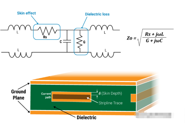
(4) Poor impedance
Impedance is an important indicator related to the RF performance of mobile phone boards. The common problem is that the impedance difference between PCB batches is relatively large.
Since the impedance test strip is generally made on the edge of the large PCB board and will not be shipped with the board, the supplier can be asked to provide the impedance strip and test report of the batch for reference every time it ships.
At the same time, it is also required to provide comparative data of the board edge wire diameter and the board inner wire diameter.
(5) Solder mask blistering/peeling off
This type of problem is usually caused by abnormal control of the PCB solder mask process, or the selection of inappropriate solder mask ink (cheap, non-metallic gold ink, not suitable for mounting flux), or it may be caused by too high temperature of mounting and reworking. To prevent batch problems, PCB suppliers need to formulate corresponding reliability test requirements and control them at different stages.
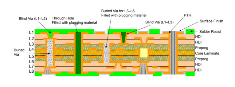
(6) Poor plugging
Poor plugging is mainly caused by insufficient technical capabilities of PCB factories or simplified processes. It is manifested as incomplete plugging, copper exposure or false copper exposure in the hole ring. It may cause insufficient solder, short circuit with the patch or assembled device, residual impurities in the hole, etc. This problem can be found in the appearance inspection, so it can be controlled in the incoming material inspection and the PCB factory is required to make improvements.
GET PCB MANUFACTURING AND ASSEMBLY QUOTE NOW!
2. Methods for judging the quality of PCB boards
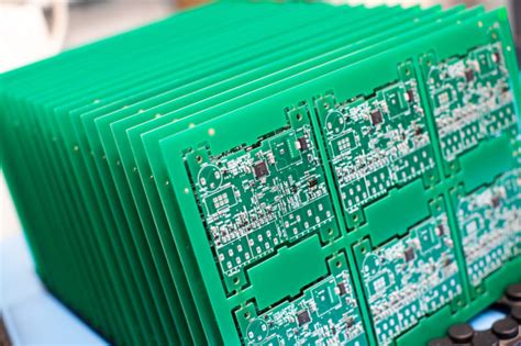
(1). The size and thickness of the PCB board must be consistent with the specified appearance size and thickness, and there must be no deviation. The surface of the circuit board is free of defects, deformation, shedding, scratches, open circuits, short circuits, white oxidation, yellowing, uncleanness or excessive etching marks, dirt, copper particles and other impurities.
(2). The ink coverage is uniform and bright, without peeling, scratches, copper exposure, deviation, printing plate and other phenomena.
(3). The symbols and letters in the screen printing are clear, without omissions and blurs, reversals, deviations and other undesirable phenomena.
(4). The carbon film shall not have defects, deviations, short circuits, open circuits, reverse printing and other phenomena.
(5). The PCB bottom plate is formed without leakage, deviation, hole collapse, flashing, plugging, beer explosion, beer reverse, crushing and other phenomena.
(6). Is the edge of the PCB smooth? If it is a V-shaped cutting process, pay attention to whether the V-shaped cutting groove causes wire breakage, whether the two sides are symmetrical, etc.
GET PCB AND ASSEMBLY SERVICE QUOTE NOW!
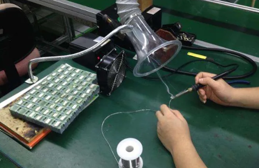
3. What are the reasons that affect the welding quality of PCB circuit boards?
(1) The design of the PCB affects the welding quality. If the PCB size is too large, although welding is easier to control, the printed lines are long, the impedance increases, the anti-noise ability decreases, and the cost increases;
if it is too small, the heat dissipation decreases, the welding is difficult to control, and adjacent lines are prone to mutual interference. Therefore, the PCB board design must be optimized.
(2) The solderability of the circuit board hole affects the welding quality. The so-called solderability refers to the property of the metal surface being wetted by the molten solder, that is, the metal surface where the solder is located forms a relatively uniform and continuous layer of light. Smooth attachment film.
If the solderability of the circuit board hole is poor, it will cause cold soldering defects, affect the parameters of the components in the circuit, cause unstable conduction between the components and the inner layer wires, and cause the entire circuit to fail.
(3) Welding defects caused by warping
Warping is often caused by temperature imbalance between the upper and lower parts of the PCB. The PCB and components warp during the welding process, and defects such as cold soldering and short circuits occur due to stress deformation.
At the same time as the PCB warps, the components themselves may also warp, and the solder joints located in the center of the components are lifted off the PCB, resulting in empty solder joints. This often occurs when only flux is used without solder paste to fill the gaps. When solder paste is used, the solder paste and the solder balls are connected together due to deformation to form a short circuit defect.