PCB Reverse Engineering: Techniques, Applications, and Ethical Considerations
Introduction
Printed Circuit Board (PCB) reverse engineering is the process of analyzing an existing PCB to understand its design, functionality, and components without access to original schematics or documentation. This practice is widely used in industries such as electronics repair, legacy system maintenance, competitive analysis, and security testing. While PCB reverse engineering can be a valuable tool for innovation and troubleshooting, it also raises ethical and legal concerns, particularly when used for cloning proprietary designs or intellectual property theft.
This article explores the techniques, applications, challenges, and ethical considerations of PCB reverse engineering. We will discuss the step-by-step process, tools used, real-world applications, and the legal framework surrounding this practice.
1. The PCB Reverse Engineering Process
Reverse engineering a PCB involves several systematic steps to extract design information from a physical board. The key stages include:
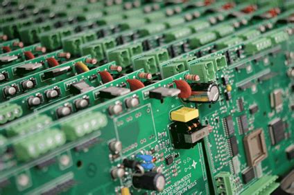
1.1 Visual Inspection and Documentation
The first step is a thorough visual examination of the PCB to identify:
- Components: Resistors, capacitors, ICs, connectors, etc.
- Layers: Determining if the PCB is single-sided, double-sided, or multi-layered.
- Traces and Vias: Tracking copper pathways that connect components.
- Power and Ground Planes: Identifying voltage distribution networks.
High-resolution cameras and microscopes are often used to document the board layout before disassembly.
1.2 PCB Depaneling and Layer Separation
For multi-layer PCBs, reverse engineering requires layer separation. Techniques include:
- Mechanical Sanding: Gradually sanding down layers to expose inner traces.
- Chemical Etching: Using solvents to dissolve epoxy and reveal conductive layers.
- X-ray Imaging: Non-destructive method to visualize internal traces (common in high-security applications).
1.3 Trace Mapping and Schematic Reconstruction
After layer analysis, engineers manually or digitally map the connections between components. This involves:
- Manual Tracing: Using a multimeter to verify connectivity.
- Automated Scanning: Optical scanners or specialized software convert PCB images into digital schematics.
- Schematic Generation: Tools like KiCad, Altium, or OrCAD help reconstruct the circuit diagram.
1.4 Component Identification and BOM Extraction
Identifying each component is crucial for replication or repair. Engineers:
- Decode Markings: ICs, resistors, and capacitors have codes that reveal specifications.
- Cross-Reference Datasheets: Matching components with manufacturer details.
- Generate a Bill of Materials (BOM): Listing all parts for reproduction.
1.5 Functional Analysis and Testing
Once the schematic is reconstructed, engineers test the PCB to verify functionality:
- Power-Up Testing: Checking for correct voltage levels and signal integrity.
- Signal Probing: Using oscilloscopes and logic analyzers to validate circuit behavior.
- Firmware Extraction (if applicable): Dumping microcontroller code for further analysis.
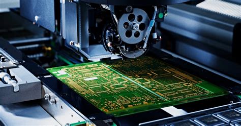
2. Tools and Techniques for PCB Reverse Engineering
Several tools and methodologies assist in PCB reverse engineering:
2.1 Hardware Tools
- Microscopes & Magnifiers: For detailed inspection of small components.
- Multimeters & Oscilloscopes: For electrical testing.
- X-ray & CT Scanners: For non-destructive internal analysis.
- Desoldering Stations: For removing components without damage.
2.2 Software Tools
- PCB Design Software: Altium, KiCad, Eagle (for schematic recreation).
- Image Processing Tools: Photoshop, GIMP (for enhancing PCB images).
- Automated Tracing Software: ScanCAD, PCB Reverse Engineering Suite.
- Firmware Analysis Tools: Ghidra, IDA Pro (for embedded systems).
2.3 Advanced Techniques
- Automated Optical Inspection (AOI): AI-assisted trace recognition.
- 3D Scanning: For complex multi-layer boards.
- Electromagnetic Analysis: Detecting signal leaks for security testing.
3. Applications of PCB Reverse Engineering
PCB reverse engineering serves multiple legitimate purposes:
3.1 Legacy System Maintenance
Many older electronic systems lack documentation. Reverse engineering helps:
- Repair obsolete military, aerospace, or industrial equipment.
- Replace discontinued components with modern equivalents.
3.2 Competitive Analysis & Benchmarking
Companies analyze competitor products to:
- Understand design innovations.
- Improve their own products without infringing patents.
3.3 Security Research & Vulnerability Assessment
Cybersecurity experts use reverse engineering to:
- Identify hardware backdoors in critical systems.
- Test IoT devices for vulnerabilities.
3.4 Counterfeit Detection & Quality Control
Manufacturers verify third-party PCBs to:
- Detect counterfeit components.
- Ensure compliance with design specifications.
3.5 Academic & Research Purposes
Universities and researchers study PCB designs to:
- Teach electronics design principles.
- Develop new reverse engineering methodologies.
4. Challenges in PCB Reverse Engineering
Despite its benefits, PCB reverse engineering presents several challenges:
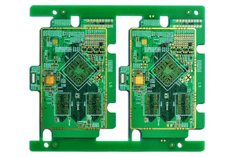
4.1 Complexity of Multi-Layer Boards
Modern PCBs can have 10+ layers, making trace mapping difficult.
4.2 Encrypted or Obsolete Components
Some ICs have proprietary firmware or are no longer available.
4.3 Legal and Ethical Risks
Unauthorized reverse engineering may violate:
- Patents & Copyrights: Copying protected designs.
- Trade Secrets: Extracting confidential schematics.
- DMCA (Digital Millennium Copyright Act): Bypassing DRM protections.
4.4 Time and Cost Constraints
Manual reverse engineering is labor-intensive and expensive for complex boards.
5. Ethical and Legal Considerations
The legality of PCB reverse engineering varies by jurisdiction. Key considerations include:
5.1 Permissible Cases (Fair Use)
- Repair & Interoperability: Fixing devices without schematics.
- Academic Research: Non-commercial study.
- Security Testing: Ethical hacking with permission.
5.2 Prohibited Cases (IP Violation)
- Cloning for Profit: Selling counterfeit PCBs.
- Military Espionage: Stealing defense technology.
- Circumventing DRM: Illegal under DMCA.
5.3 Best Practices for Ethical Reverse Engineering
- Obtain Legal Advice: Ensure compliance with local laws.
- Document Justification: Prove legitimate use (e.g., repair, research).
- Avoid Distribution of Proprietary Data: Do not share copyrighted schematics.
6. Conclusion
PCB reverse engineering is a powerful technique with applications in repair, security, and innovation. While it enables the restoration of legacy systems and detection of vulnerabilities, it must be conducted ethically to avoid legal repercussions. As PCBs become more complex, automated tools and AI-assisted analysis will play a larger role in streamlining the process. Engineers and researchers must balance technological exploration with respect for intellectual property rights to ensure responsible use of reverse engineering methodologies.
By understanding the techniques, challenges, and legal frameworks, professionals can leverage PCB reverse engineering as a tool for progress rather than exploitation.


