PCB Screen Printing: Process, Techniques, and Applications
Introduction
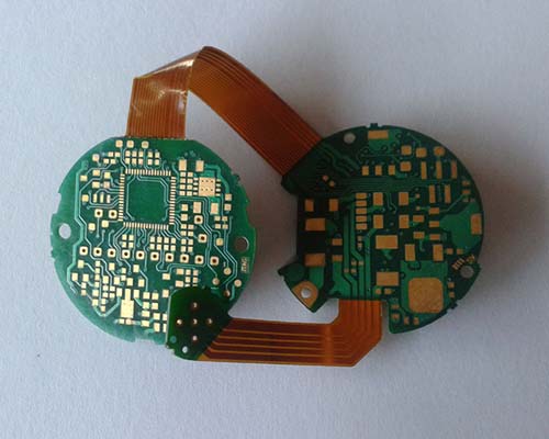
Printed Circuit Boards (PCBs) are essential components in modern electronics, providing mechanical support and electrical connections for electronic components. One critical step in PCB manufacturing is screen printing, also known as silk screening, which involves applying labels, markings, and identifiers onto the PCB surface. This process ensures proper component placement, assembly guidance, and traceability.
This article explores the PCB screen printing process, including its techniques, materials, advantages, challenges, and applications in the electronics industry.
1. What is PCB Screen Printing?
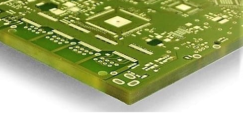
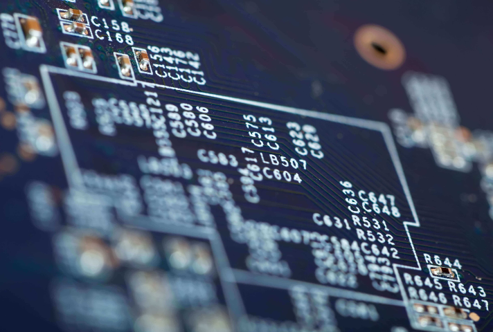
Screen printing is a technique used to apply ink onto a PCB’s surface to create component labels, logos, reference designators, and other markings. These markings help technicians and automated machines correctly assemble and troubleshoot PCBs.
Key Functions of PCB Screen Printing:
- Component Identification: Labels such as R1 (Resistor), C2 (Capacitor), U3 (IC) guide assembly.
- Polarity Indicators: Marks for diodes, capacitors, and IC orientation.
- Manufacturer Information: Company logos, part numbers, and certifications.
- Safety & Compliance: Warning symbols, UL marks, and RoHS compliance labels.
Screen printing is typically performed after soldermask application but before surface finish and component assembly.
2. PCB Screen Printing Process
Step 1: Design & Stencil Preparation
- The PCB design software (e.g., Altium, KiCad, Eagle) generates a silkscreen layer containing text and symbols.
- A stencil (screen mesh) is created, usually made of polyester or stainless steel, with openings corresponding to the desired markings.
Step 2: Ink Selection
The most common inks used in PCB screen printing are:
- Epoxy-Based Inks: Durable and resistant to heat, chemicals, and abrasion.
- UV-Curable Inks: Dry quickly under UV light, improving production speed.
- Thermosetting Inks: Require heat curing for long-lasting adhesion.
Step 3: Printing Process
- The PCB is placed on a flat surface or conveyor belt.
- The screen stencil is aligned over the PCB.
- Ink is applied and spread using a squeegee, forcing ink through the stencil openings onto the PCB.
- The PCB is cured (via UV light or heat) to harden the ink.
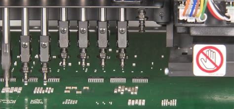
Step 4: Inspection & Quality Control
- Automated Optical Inspection (AOI) checks for misprints, smudging, or incomplete markings.
- Manual verification ensures readability and alignment accuracy.

3. Screen Printing Techniques
A. Manual Screen Printing
- Used for prototyping or low-volume production.
- Operators manually align the stencil and apply ink.
- Cost-effective but less precise than automated methods.
B. Automated Screen Printing
- High-speed machines handle mass production.
- Precise alignment with vision systems ensures consistency.
- Suitable for high-density PCBs with fine markings.
C. Direct Legend Printing (DLP)
- An alternative to traditional screen printing.
- Uses inkjet printing to apply markings directly onto the PCB.
- No stencil required, allowing for quick design changes.
4. Advantages of PCB Screen Printing
✅ Cost-Effective: Lower setup costs compared to laser marking.
✅ High Durability: Resistant to heat, chemicals, and mechanical wear.
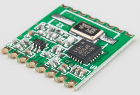
✅ Versatility: Works on various PCB materials (FR4, flexible PCBs, metal-core PCBs).
✅ Clear Identification: Improves assembly accuracy and troubleshooting.
5. Challenges & Limitations
❌ Limited Resolution: Fine-pitch components may require alternative methods like LPI (Liquid Photo Imaging).
❌ Ink Smudging: Poor curing or handling can cause defects.
❌ Alignment Issues: Misregistration can occur if the stencil is not properly aligned.
6. Applications of PCB Screen Printing
A. Consumer Electronics
- Smartphones, laptops, and wearables use screen printing for branding and assembly guidance.
B. Automotive Electronics
- PCBs in engine control units (ECUs) and infotainment systems require durable markings.
C. Industrial & Medical Devices
- High-reliability PCBs in medical equipment need clear, long-lasting labels.
D. Aerospace & Defense
- Military-grade PCBs use screen printing for traceability and compliance.
7. Future Trends in PCB Screen Printing
🔹 Higher Precision: Advances in stencil manufacturing enable finer details.
🔹 Eco-Friendly Inks: Water-based and lead-free inks for sustainable production.
🔹 Hybrid Printing: Combining screen printing with inkjet or laser marking for flexibility.
Conclusion
PCB screen printing remains a vital process in electronics manufacturing, offering a balance of cost, durability, and functionality. While newer technologies like inkjet and laser marking are emerging, screen printing continues to dominate due to its reliability and efficiency.
As PCBs become smaller and more complex, advancements in ink formulations, automation, and printing techniques will ensure that screen printing remains a key player in the industry.
By understanding the process, materials, and best practices, manufacturers can optimize screen printing for high-quality PCB production.