PCB signal line layout
Before starting the circuit design of the PCB, find out the key signals based on relevant knowledge and analyze those key signals. For example, in this application note, for the most critical signals, such as clock signals, switch signals and other switching signals, one or more of the following measures can be adopted.
1. Line termination
According to [5], circuit designers can choose many different termination technologies. For long lines, line termination can avoid emission, and for short lines, line termination can avoid ringing, so it is necessary. Most of them are terminal termination and source termination. For example, terminal termination minimizes the rise time, so it is suitable for speed optimization. Source end serial termination can reduce the current of the signal track, so it can better reduce radiation.
The series termination resistor must be as close to the signal driver (source) as possible. It can be optimized to match the transmission line impedance or form a low-pass filter with the load capacitor. The transmission line impedance should match the sum of the driving impedances and the resistor value should be equal to the transmission line impedance. In order to achieve EME optimization, the current on the signal line and the harmonics of the signal frequency should be minimized. Therefore, it is desirable to obtain a resistor as large as the timing and functional constraints allow.
2.Transmission lines on PCBs
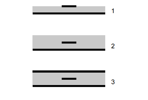
The most common transmission lines used on PCBs are striplines or microstrip lines. In [5], complex and accurate formulas for calculating impedance, delay, etc. are available. As shown in Figure 5-11, Figures 1 and 2 are examples of microstrip lines; Figure 3 is an example of stripline. It is worth noting that when calculating striplines or microstrip lines, the parameters are assumed to be on an infinite ground. Since this is not a true ground plane, the signal line is at least 5 times the larger of the line width and line spacing. Another reason for implementing this measure is to implement a guard ring so that routing can be done at the edge of the board.
When implementing stripline or microstrip, confirm that the above assumptions are met during the PCB design process. Any local crosstalk from other lines can affect the characteristics of the stripline or microstrip and may cause unintentional high radiation. In addition, the power plane is not suitable as a reference plane for stripline or microstrip.
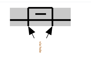
For the stackup, the distance between all layers of the PCB should be carefully considered and defined. The distance to the ground and the thickness of the material will affect the characteristics of the trace. Further, the signal radiation on the ground is proportional to the distance from the signal on the ground to the ground. Therefore, any critical signal on the ground should not be more than 0.2mm away from the ground, and the clock frequency above 30MHz should not be more than 0.1mm away from the ground. The clock frequency above 50MHz should be treated as a stripline instead.
If there are only a few strip lines, it is possible to avoid using a second ground plane because it can be replaced by a ground line. For this purpose, the clock signal should be routed on a layer close to the ground, and a wider ground line should be placed on top of the clock signal on the next layer. This ground line is connected to both sides of the clock signal every 5-10 mm. Figure 5-12 gives an example of a 4-layer board.