PCB Simulation Analysis: Techniques, Tools, and Best Practices
1. Introduction
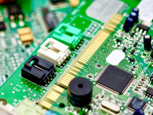
Printed Circuit Board (PCB) design is a critical aspect of modern electronics, influencing performance, reliability, and manufacturability. As PCBs become more complex with higher signal speeds, increased power densities, and miniaturized components, simulation analysis has become indispensable. PCB simulation allows engineers to predict and optimize electrical, thermal, and mechanical behavior before physical prototyping, reducing development costs and time-to-market.
This article explores the key aspects of PCB simulation analysis, including:
- Types of PCB simulations (signal integrity, power integrity, thermal analysis, EMI/EMC)
- Popular simulation tools
- Best practices for effective PCB simulation
- Future trends in PCB simulation
2. Types of PCB Simulation Analysis
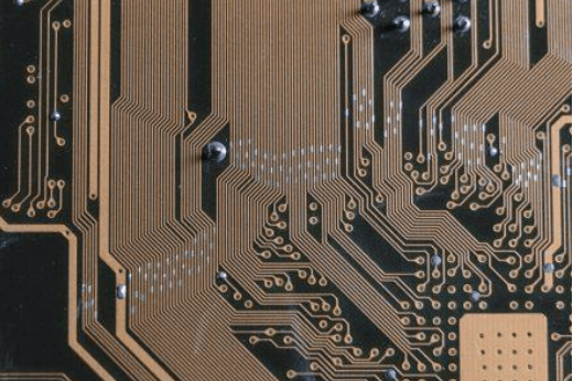
2.1 Signal Integrity (SI) Analysis
Signal integrity ensures that electrical signals propagate correctly across PCB traces without distortion. Key challenges include:
- Reflections (due to impedance mismatches)
- Crosstalk (unwanted coupling between traces)
- Signal attenuation (losses in high-frequency signals)
Simulation Techniques:
- Time-domain reflectometry (TDR) – Identifies impedance discontinuities.
- Eye diagram analysis – Evaluates signal quality in high-speed digital circuits.
- S-parameter modeling – Analyzes frequency-dependent behavior.
Common Tools: Ansys SIwave, Cadence Sigrity, Keysight ADS.
2.2 Power Integrity (PI) Analysis
Power integrity ensures stable voltage delivery across the PCB. Issues include:
- Voltage drops (IR drop) – Due to trace resistance.
- Power plane resonance – Causing noise in power distribution networks (PDNs).
- Decoupling capacitor optimization – To suppress high-frequency noise.
Simulation Techniques:
- DC analysis – Checks IR drop.
- AC analysis – Evaluates impedance of PDN.
- Transient analysis – Simulates dynamic load conditions.
Common Tools: Cadence Allegro PI, Ansys RedHawk, Synopsys PrimePower.
2.3 Thermal Analysis
Excessive heat can degrade component performance and reliability. Thermal simulation helps:
- Identify hotspots.
- Optimize heat sinks and airflow.
- Prevent thermal-induced failures.
Simulation Techniques:
- Conduction/convection analysis – Models heat dissipation.
- Thermal stress analysis – Predicts warpage due to temperature changes.
Common Tools: Ansys Icepak, Siemens FloTHERM, COMSOL Multiphysics.
2.4 Electromagnetic Interference/Compatibility (EMI/EMC) Analysis
EMI/EMC simulations ensure PCBs comply with regulatory standards by minimizing:
- Radiated emissions (unintended RF radiation).
- Conducted emissions (noise through power lines).
- Susceptibility to external interference.
Simulation Techniques:
- Near-field/far-field analysis – Predicts radiation patterns.
- Shielding effectiveness evaluation – Assesses enclosure performance.
Common Tools: CST Studio Suite, Altair FEKO, Ansys HFSS.
3. Popular PCB Simulation Tools
Several software tools are widely used in PCB simulation:
| Tool | Key Features | Use Cases |
|---|---|---|
| Ansys HFSS | 3D EM simulation | High-frequency SI, EMI |
| Cadence Sigrity | PI/SI analysis | Power-aware signal integrity |
| Keysight ADS | High-speed digital SI | RF/microwave design |
| Siemens HyperLynx | SI/PI/thermal | Multi-domain analysis |
| COMSOL Multiphysics | Thermal/structural | Coupled physics simulations |
4. Best Practices for PCB Simulation
To maximize simulation accuracy and efficiency, engineers should follow these best practices:
4.1 Model Fidelity
- Use accurate component models (SPICE, IBIS, S-parameters).
- Include parasitic effects (via inductance, trace resistance).
4.2 Meshing and Solvers
- Apply adaptive meshing for high-frequency simulations.
- Choose appropriate solvers (FEM, FDTD, MoM) based on the problem.
4.3 Validation and Correlation
- Compare simulation results with lab measurements.
- Perform sensitivity analysis to identify critical parameters.
4.4 Simulation Workflow Integration
- Link schematic design (e.g., Altium, Cadence) with simulation tools.
- Automate repetitive tasks using scripting (Python, MATLAB).
5. Future Trends in PCB Simulation
Emerging technologies are shaping the future of PCB simulation:
5.1 AI/ML-Driven Optimization
- Machine learning accelerates parameter tuning and failure prediction.
- Neural networks reduce simulation time for complex scenarios.
5.2 Cloud-Based Simulation
- Enables distributed computing for large-scale simulations.
- Facilitates collaboration across global teams.
5.3 Multi-Physics Co-Simulation
- Integrates electrical, thermal, and mechanical analysis in a unified environment.
- Essential for advanced packaging (3D ICs, chiplets).
5.4 Quantum and High-Frequency Design
- Simulations for THz and quantum computing PCBs require new modeling approaches.
6. Conclusion
PCB simulation analysis is a cornerstone of modern electronics design, enabling engineers to predict and mitigate issues before fabrication. By leveraging advanced SI, PI, thermal, and EMI simulations, designers can achieve first-pass success, reduce costs, and accelerate product development. As AI, cloud computing, and multi-physics simulations evolve, PCB design will become even more efficient and reliable.
For engineers, staying updated with the latest simulation tools and methodologies is crucial to maintaining a competitive edge in the fast-evolving electronics industry.