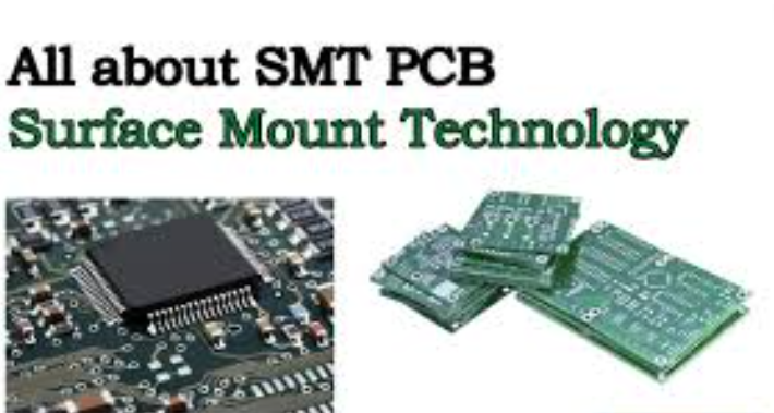
Pcb smt
Understanding The Basics Of PCB SMT Assembly
Printed Circuit Board Surface Mount Technology (PCB SMT) assembly is a cornerstone of modern electronics manufacturing, enabling the production of compact, efficient, and reliable electronic devices.
Understanding the basics of PCB SMT assembly is essential for anyone involved in the design, production, or utilization of electronic components. This article aims to elucidate the fundamental aspects of PCB SMT assembly, providing a comprehensive overview of the process and its significance.
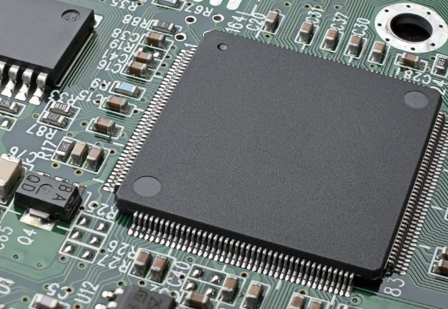
To begin with, Surface Mount Technology (SMT) refers to the method of mounting electronic components directly onto the surface of a printed circuit board (PCB).
Unlike traditional through-hole technology, which requires drilling holes into the PCB for component leads, SMT allows for components to be placed on both sides of the board, significantly increasing the density and complexity of the circuits that can be created. This advancement has been pivotal in the miniaturization of electronic devices, from smartphones to medical equipment.
The PCB SMT assembly process involves several critical steps, each requiring precision and expertise.
Initially, the PCB is prepared by applying a layer of solder paste to the areas where components will be mounted. This is typically done using a stencil that ensures the paste is applied accurately and consistently. The solder paste itself is a mixture of tiny solder balls and flux, which helps to clean the surfaces and improve the soldering process.
Following the application of solder paste, the next step is the placement of components.
This is achieved using automated machines known as pick-and-place machines, which are capable of placing thousands of components per hour with remarkable accuracy. These machines use a combination of vacuum nozzles and vision systems to pick up components from reels or trays and place them onto the PCB in the exact locations specified by the design.
Once all components are placed, the PCB undergoes a reflow soldering process.
During reflow soldering, the board is passed through a controlled heating environment, typically an oven, where the solder paste melts and forms a solid connection between the components and the PCB. The temperature profile of the oven is carefully controlled to ensure that the solder melts and solidifies correctly without damaging the components or the board.
After reflow soldering, the assembled PCB is inspected to ensure that all components are correctly placed and soldered.
This inspection can be performed using automated optical inspection (AOI) systems, which use cameras and image processing software to detect any defects. In some cases, X-ray inspection may also be used to examine solder joints that are not visible to the naked eye, such as those beneath ball grid array (BGA) components.
The final step in the PCB SMT assembly process is testing.
Functional testing ensures that the assembled PCB operates as intended, with all electrical connections and components performing correctly. This may involve a variety of tests, including in-circuit testing (ICT), which checks the electrical performance of individual components, and functional testing, which verifies the overall operation of the assembled device.
In conclusion, PCB SMT assembly is a sophisticated and highly efficient method for producing electronic circuits. Its ability to accommodate high component densities and complex designs has made it indispensable in the electronics industry. By understanding the basics of this process, one can appreciate the precision and expertise required to produce the advanced electronic devices that are integral to modern life.
Top Trends In PCB SMT Technology For 2023
In 2023, the landscape of Printed Circuit Board Surface Mount Technology (PCB SMT) continues to evolve, driven by advancements in technology and the ever-increasing demand for more efficient, compact, and reliable electronic devices.
One of the most significant trends in PCB SMT technology is the miniaturization of components.
As consumer electronics become smaller and more powerful, the need for compact and efficient PCB designs has never been greater. This trend is pushing the boundaries of what is possible in terms of component placement and soldering techniques, necessitating the development of more precise and reliable SMT equipment.
Another notable trend is the increasing adoption of automation and artificial intelligence (AI) in the PCB SMT process.
Automation has long been a part of PCB manufacturing, but recent advancements in AI and machine learning are taking it to new heights. AI-driven systems can now optimize the placement of components, predict potential defects, and even adjust the manufacturing process in real-time to ensure the highest quality output. This not only improves efficiency but also significantly reduces the likelihood of errors, leading to higher yields and lower production costs.
In addition to automation, the integration of advanced materials is also shaping the future of PCB SMT technology.
High-performance materials such as flexible substrates and advanced solder pastes are becoming more prevalent, enabling the production of more durable and versatile PCBs. These materials offer improved thermal management, better electrical performance, and greater mechanical strength, making them ideal for a wide range of applications, from consumer electronics to industrial and automotive systems.
Moreover, the rise of the Internet of Things (IoT) is driving the need for more sophisticated PCB designs.
IoT devices often require complex, multi-layer PCBs with a high density of components. This has led to the development of new design and manufacturing techniques that can accommodate these requirements. For instance, the use of 3D printing in PCB manufacturing is gaining traction, allowing for the creation of intricate and highly customized PCB designs that were previously impossible to achieve with traditional methods.
Sustainability is another critical trend in PCB SMT technology for 2023.
As environmental concerns become more pressing, the electronics industry is under increasing pressure to adopt more sustainable practices. This includes the use of eco-friendly materials, reducing waste, and improving energy efficiency throughout the manufacturing process. Companies are investing in research and development to create more sustainable PCB solutions, such as biodegradable substrates and lead-free soldering techniques, which not only reduce environmental impact but also comply with stringent regulatory requirements.
Furthermore, the demand for higher data rates and faster processing speeds is driving innovations in PCB SMT technology.
The advent of 5G and other high-speed communication technologies requires PCBs that can handle higher frequencies and greater data throughput. This has led to the development of advanced signal integrity solutions and high-speed interconnects, which are essential for maintaining performance and reliability in these demanding applications.
In conclusion, the top trends in PCB SMT technology for 2023 reflect a dynamic and rapidly evolving industry. From miniaturization and automation to advanced materials and sustainability, these trends are shaping the future of PCB manufacturing. As technology continues to advance, the PCB SMT industry will undoubtedly continue to innovate, meeting the ever-growing demands for more efficient, reliable, and sustainable electronic devices.
Common Challenges In PCB SMT Manufacturing And How To Overcome Them
Printed Circuit Board Surface Mount Technology (PCB SMT) manufacturing is a critical process in the electronics industry, enabling the production of compact, high-performance electronic devices. However, this process is not without its challenges. Understanding these common issues and implementing effective solutions is essential for ensuring the reliability and efficiency of PCB SMT manufacturing.
One of the primary challenges in PCB SMT manufacturing is solder paste application.
Solder paste must be applied with precision to ensure proper component attachment and electrical connectivity. Inconsistent solder paste deposition can lead to defects such as solder bridges, insufficient solder joints, and tombstoning. To overcome this, manufacturers can employ advanced stencil printing techniques and regularly inspect and maintain stencils to ensure uniform paste application. Additionally, automated optical inspection (AOI) systems can be used to detect and correct any inconsistencies early in the process.
Another significant challenge is component placement accuracy.
With the increasing miniaturization of electronic components, precise placement is more critical than ever. Misaligned components can result in poor solder joints and functional failures. To address this, manufacturers can utilize high-precision pick-and-place machines equipped with vision systems that ensure accurate component alignment. Regular calibration and maintenance of these machines are also crucial to maintaining their accuracy over time.
Thermal management during the reflow soldering process presents another common challenge.
The reflow process involves heating the entire PCB assembly to melt the solder paste and form reliable solder joints. However, improper thermal profiles can lead to issues such as solder voids, component warping, and thermal stress. To mitigate these risks, manufacturers should carefully design and control the reflow oven profiles, taking into account the thermal characteristics of both the components and the PCB material. Using thermal profiling tools to monitor and adjust the temperature gradients can help achieve optimal soldering results.
Component handling and storage also pose challenges in PCB SMT manufacturing.
Moisture-sensitive components can absorb moisture from the environment, leading to defects such as popcorning during the reflow process. To prevent this, manufacturers should implement strict moisture control measures, including proper storage in dry cabinets and the use of desiccant materials. Additionally, handling components with care and using anti-static precautions can prevent damage from electrostatic discharge (ESD), which can compromise component functionality.
Quality control is another critical aspect that can present challenges in PCB SMT manufacturing.
Ensuring the final product meets the required specifications and standards is paramount. Implementing a robust quality control system that includes AOI, X-ray inspection, and in-circuit testing (ICT) can help identify and rectify defects at various stages of the manufacturing process. Continuous monitoring and feedback loops can also drive process improvements and reduce the occurrence of defects.
Finally, supply chain management can impact PCB SMT manufacturing.
Delays or inconsistencies in the supply of components can disrupt production schedules and lead to increased costs. Establishing strong relationships with reliable suppliers and maintaining adequate inventory levels can mitigate these risks. Additionally, adopting a flexible manufacturing approach that can accommodate changes in component availability can enhance resilience against supply chain disruptions.
In conclusion, while PCB SMT manufacturing presents several challenges, understanding these issues and implementing effective solutions can significantly enhance the reliability and efficiency of the process. By focusing on precise solder paste application, accurate component placement, proper thermal management, careful component handling, robust quality control, and efficient supply chain management, manufacturers can overcome these challenges and produce high-quality electronic devices.
The Future Of PCB SMT: Innovations And Advancements
The future of Printed Circuit Board Surface Mount Technology (PCB SMT) is poised for significant advancements, driven by the relentless pace of technological innovation and the ever-increasing demand for more efficient, compact, and reliable electronic devices. As we delve into the future of PCB SMT, it is essential to consider the various innovations and advancements that are shaping this critical aspect of electronics manufacturing.
One of the most notable trends in PCB SMT is the miniaturization of components.
As electronic devices become smaller and more powerful, the need for compact and efficient PCB designs has never been greater. This trend is pushing the boundaries of what is possible in terms of component placement and soldering techniques. Advanced placement machines, capable of handling components as small as 01005 (0.4mm x 0.2mm), are becoming increasingly common. These machines offer unparalleled precision and speed, ensuring that even the tiniest components are accurately placed on the PCB.
In addition to miniaturization, the integration of advanced materials is another key area of innovation in PCB SMT.
High-performance materials, such as flexible substrates and advanced laminates, are being developed to meet the demands of modern electronic devices. These materials offer improved thermal management, enhanced signal integrity, and greater mechanical flexibility, making them ideal for applications in industries such as aerospace, automotive, and medical devices. The use of these advanced materials is enabling the creation of more robust and reliable PCBs, capable of withstanding the rigors of harsh environments and demanding applications.
Moreover, the advent of Industry 4.0 and the Internet of Things (IoT) is revolutionizing the PCB SMT landscape.
The integration of smart manufacturing technologies, such as artificial intelligence (AI), machine learning, and big data analytics, is transforming the way PCBs are designed, manufactured, and tested. AI-powered design tools are enabling engineers to optimize PCB layouts for performance, manufacturability, and cost. Machine learning algorithms are being used to predict and prevent defects in the manufacturing process, ensuring higher yields and lower production costs. Big data analytics is providing manufacturers with valuable insights into production trends and equipment performance, allowing for more informed decision-making and continuous improvement.
Furthermore, advancements in soldering techniques are playing a crucial role in the future of PCB SMT.
Traditional soldering methods, such as wave soldering and reflow soldering, are being enhanced with new technologies that offer greater precision and reliability. For instance, laser soldering is gaining traction as a method for achieving high-quality solder joints with minimal thermal stress on components. This technique uses focused laser beams to selectively heat solder joints, resulting in faster and more accurate soldering processes. Additionally, the development of lead-free solder alloys is addressing environmental and health concerns associated with traditional lead-based solders, while still providing reliable and durable connections.
Lastly, the push towards sustainability is influencing the future of PCB SMT.
Manufacturers are increasingly adopting eco-friendly practices, such as using recyclable materials, reducing waste, and minimizing energy consumption. These efforts are not only beneficial for the environment but also contribute to cost savings and improved efficiency in the manufacturing process.
In conclusion, the future of PCB SMT is characterized by a myriad of innovations and advancements that are driving the industry forward. From miniaturization and advanced materials to smart manufacturing technologies and improved soldering techniques, these developments are paving the way for more efficient, reliable, and sustainable electronic devices. As the demand for cutting-edge electronics continues to grow, the PCB SMT industry will undoubtedly continue to evolve, embracing new technologies and methodologies to meet the challenges of tomorrow.


